BuMa_2010_04 - Deutsche Bunsengesellschaft für Physikalische ...
BuMa_2010_04 - Deutsche Bunsengesellschaft für Physikalische ...
BuMa_2010_04 - Deutsche Bunsengesellschaft für Physikalische ...

Sie wollen auch ein ePaper? Erhöhen Sie die Reichweite Ihrer Titel.
YUMPU macht aus Druck-PDFs automatisch weboptimierte ePaper, die Google liebt.
DEUTSCHE BUNSEN-GESELLSCHAFT<br />
domains, indicated in green, each of which gives rise to a separate<br />
set of diffraction spots. The p(√7 x √7) R19° superstructure<br />
has a three-fold rotation symmetry but does not share the<br />
mirror symmetry plane with the substrate (dashed line) this<br />
leads to an extra mirror domain, again indicated in green, with<br />
a set of extra diffraction spots.<br />
If the adsorbate coverage is known from other methods, as<br />
in the present example, it is straight forward to work out the<br />
number of molecules per unit cell: there is one molecule in the<br />
p(√3 x √3) R30° unit cell (coverage 1/3), two in the c(2 x 4)<br />
(coverage 2/4) and four molecules in the p(√7 x √7) R19° unit<br />
cell (coverage 4/7).<br />
The diffraction spots of the p(√3 x √3) R30° pattern are signifi<br />
cantly broader than those of the other structures. This indicates<br />
that the ordered domains are considerably smaller than<br />
the coherence or transfer width of the LEED system. The radial<br />
spot width is about 1/5 of the length of the reciprocal lattice<br />
vectors, therefore the corresponding width of the domains is<br />
on average about fi ve unit cells or 2 nm.<br />
4.2 SPOT PROFILES<br />
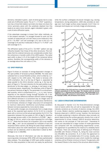
Figure 6 shows an example of energy-dependent changes in<br />
the spot profi les of terraced surfaces [Woll98]. The data were<br />
collected from a vicinal Pd{100} surface, which is tilted by 1.1°<br />
with respect to the (100) plane. This leads to terraces with<br />
(100) orientation, like in at the top of Figure 1, separated by<br />
steps parallel to the [011] direction (vector a 1 in the top diagram<br />
of Figure 1). The scan direction for the spot profi les is perpendicular<br />
to the step edges, i.e. along a 2 in real space or a 2*<br />
in reciprocal space, respectively. The abscissa units of Figure 6<br />
are percent fractions of |a 2*|. The parameter S is a dimensionless<br />
quantity, which is proportional to k z,out (n 1,n 2) and, hence,<br />
depends on the electron energy through Equation (6). S describes<br />
the phase difference between electron waves emerging<br />
from different terraces in a convenient way: an integer value of<br />
S indicates the in-phase condition or constructive interference<br />
for all terraces, whereas an integer value plus 0.5 corresponds<br />
to maximum destructive interference (out-of-phase condition)<br />
between terraces separated by mono-atomic steps.<br />
The spot profi le changes very dramatically from a single sharp<br />
peak at the expected spot position (0) for S=4.0 to a double<br />
peak with a minimum at the actual spot position for S=3.5. The<br />
separation between the two peaks is 2.8% of |a 2*|, therefore<br />
the average terrace width in this direction is (0.028) -1 ∙ |a 2| =<br />
36 |a 2| or 9.8 nm, which is the value expected for a tilt angle<br />
of 1.1°. (Note that the factor 2p in Equation (10) is not needed<br />
when |Δk || | and Δw are expressed as multiples of real and<br />
reciprocal lattice vectors.) By fi tting the peak shape additional<br />
information about the width distribution and roughness of the<br />
surface can be obtained, which is described in detail by Wollschläger<br />
et al. in [Woll98].<br />
Obviously, this kind of information can also be obtained by<br />
scanning probe microscopy (STM, AFM) with less sophisticated<br />
data analysis. The advantage of LEED spot profi le analysis is<br />
that the data acquisition is fast and can easily be performed<br />
UNTERRICHT<br />
while the surface undergoes structural changes (e.g. varying<br />
temperature, during adsorption). LEED also provides an average<br />
over much larger surface areas (typically 1mm 2 ) than microscopic<br />
techniques can normally image simultaneously.<br />
Figure 6: Profiles of the (0,0) spot from a terraced (vicinal) Pd{100} surface<br />
recorded perpendicular to the step edges. The abscissa units are percent<br />
fractions of |a 2*|. Reprinted from Surface Science, 396, Wollschläger et al.,<br />
“Diffraction spot profile analysis for vicinal surfaces with long-range order”,<br />
94, Copyright (1998), with permission from Elsevier.<br />
4.3 LEED-IV STRUCTURE DETERMINATION<br />
As discussed in Section 2.3, the three-dimensional arrangement<br />
of atoms within the unit cell is responsible for the spotintensity<br />
variations as a function of electron energy, the LEED-<br />
IV curves. Modern electron scattering programs reproduce all<br />
features observed in LEED-IV curves, however, the dominance<br />
of multiple scattering in electron diffraction does normally not<br />
permit determining the surface geometry directly from a set of<br />
experimental IV curves. Instead, LEED-IV structure determination<br />
works on the principle of “trial and error”. Theoretical IV<br />
curves are calculated for a large number of model geometries<br />
and compared with the corresponding experimental curves.<br />
The agreement is quantifi ed by the means of a reliability factor<br />
or R-factor. There are several ways of defi ning such R-factors<br />
[Vanh86] with Pendry’s R-factor, R P, being the most common<br />
one [Pend80]. By convention, R P is 0 when the agreement is<br />
perfect and 1 for uncorrelated sets of IV curves. Usually, automated<br />
search procedures are used, which modify the model geometries<br />
until an R-factor minimum is found. The geometry with<br />
the lowest R-factor is the result of the structure determination.<br />
129