BuMa_2010_04 - Deutsche Bunsengesellschaft für Physikalische ...
BuMa_2010_04 - Deutsche Bunsengesellschaft für Physikalische ...
BuMa_2010_04 - Deutsche Bunsengesellschaft für Physikalische ...

Erfolgreiche ePaper selbst erstellen
Machen Sie aus Ihren PDF Publikationen ein blätterbares Flipbook mit unserer einzigartigen Google optimierten e-Paper Software.
DEUTSCHE BUNSEN-GESELLSCHAFT<br />
2.4 SPOT PROFILES<br />
While the spot positions and intensities carry information<br />
about the size and the local geometry within the surface unit<br />
cell, the spot profi le, i.e. the shape and width of a diffraction<br />
spot, is determined by the long range relative arrangement the<br />
unit cells at the surface. Vertical displacements of the surface<br />
unit cells (e.g. steps, facets) lead to split spots and changes of<br />
the spot profi le as a function of electron energy. If all surface<br />
unit cells are in the same plane (over a length of at least 10nm,<br />
which is a typical coherence width of LEED instruments), the<br />
spot profi le does not change with energy.<br />
A periodic arrangement of equal steps at the surface causes<br />
spot splitting at energies, which lead to destructive interference<br />
between electrons refl ected from adjacent terraces (“outof-phase<br />
condition”). By measuring these energies the step<br />
height can be determined directly. For a more random arrangement<br />
of steps the analysis of energy dependent changes in<br />
the spot profi les allows in many cases the determination of the<br />
mean step height and a characterization of the step distribution<br />
[Henz77,Woll98]. Facets lead to extra spots which move in<br />
k || upon changes of the kinetic energy.<br />
SmallIslands<br />
LargeIslands<br />
TerracedSurface<br />
inphase<br />
outofphase<br />
Figure 3: Effect of island size on the spot profile (top) and spot splitting<br />
induced by regular steps (bottom); in phase: constructive interference between<br />
electrons reflected from adjacent terraces; out of phase: destructive<br />
interference. (According to [Henz91]).<br />
Point defects, static disorder, and thermally induced displacements<br />
lead to an increase of the background intensity between<br />
the spots. Depending on the correlation between the scatterers,<br />
the background is either homogeneous (no correlation)<br />
or structured (correlation). If the coherently ordered surface<br />
areas (islands, domains) are small (< 10nm) and at the same<br />
vertical height, the width of these areas, Δw, is inversely proportional<br />
to the width of the LEED spots, |Δk || |:<br />
|Δk || | = 2π / Δw (10)<br />
This relation holds for each direction parallel to the surface independently.<br />
It is particularly useful for determining the size of<br />
k ||<br />
k<br />
UNTERRICHT<br />
adsorbate islands which lead to extra superstructure spots. A<br />
good introduction (in German) into spot profi le analysis is given<br />
in the book by Henzler and Göpel [Henz91].<br />
3 EXPERIMENT<br />
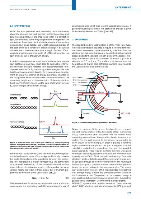
The standard modern LEED system is of the “rear view” type ,<br />
which is schematically depicted in Figure 4. The incident electron<br />
beam, accelerated by the potential V 0, is emitted from the<br />
electron gun behind a transparent hemispherical fl uorescent<br />
screen and hits the sample through a hole in the screen. Typically,<br />
the electron beam has a current of around 1 μA and a<br />
diameter of 0.5 to 1 mm. The surface is in the centre of the<br />
hemisphere so that all back-diffracted electrons travel towards<br />
the LEED screen on radial trajectories.<br />
Grid4<br />
Grid3(suppressor)<br />
Grid2(suppressor)<br />
Grid1<br />
ElectronGun<br />
V 0<br />
+56kV<br />
Screen<br />
e beam<br />
Sample<br />
Figure 4: Schematic diagram of a typical LEED instrument.<br />
(V 0 V)<br />
Before the electrons hit the screen they have to pass a retarding<br />
fi eld energy analyzer (RFA). It consists of four (sometimes<br />
three) hemispherical grids concentric with the screen, each<br />
containing a central hole, through which the electron gun is inserted.<br />
The fi rst grid (nearest to the sample) is connected to<br />
earth ground as is the sample, in order to provide a fi eld-free<br />
region between the sample and this grid. A negative potential<br />
–(V 0-ΔV) is applied to the second and third grid, the so-called<br />
suppressor grids. These repel all electrons that have undergone<br />
non-elastic scattering processes and have lost more than eΔV<br />
(typically around 5eV) of their original kinetic energy. Thus, only<br />
elastically scattered electrons and those with small energy losses<br />
can pass through to the fl uorescent screen. The fourth grid<br />
is usually on ground potential in order to reduce fi eld penetration<br />
of the screen voltage to the suppressor grids. The screen<br />
is at a potential of the order of 5-6 kV; it provides the electrons<br />
with enough energy to make the diffraction pattern visible on<br />
the fl uorescent screen. The pattern can be observed through a<br />
view-port from behind the transparent screen. Only the electron<br />
gun assembly (diameter < 15 mm) limits the view slightly.<br />
MCP-LEED systems with position sensitive “micro channel<br />
plate” (MCP) electron multipliers between the RFA grids and<br />
127