BuMa_2010_04 - Deutsche Bunsengesellschaft für Physikalische ...
BuMa_2010_04 - Deutsche Bunsengesellschaft für Physikalische ...
BuMa_2010_04 - Deutsche Bunsengesellschaft für Physikalische ...

Erfolgreiche ePaper selbst erstellen
Machen Sie aus Ihren PDF Publikationen ein blätterbares Flipbook mit unserer einzigartigen Google optimierten e-Paper Software.
DEUTSCHE BUNSEN-GESELLSCHAFT<br />
data with respect to the exact positions of atoms at a surface<br />
is somewhat more complicated and requires fully dynamical<br />
quantum mechanical scattering calculations.<br />
The use of LEED as a standard technique for surface analysis<br />
started in the early 1960’s when large enough single crystals<br />
and commercial instruments became available for surface<br />
studies. At fi rst the technique was only used for qualitative<br />
characterization of surface ordering and the identifi cation of<br />
two-dimensional superstructures. The quantitative information<br />
about the positions of the atoms within the surface is hidden<br />
in the energy-dependence of the diffraction spot intensities,<br />
the so-called LEED I-V, or I(E), curves. Computer programs and<br />
the computer power to analyze these data became available in<br />
the 1970’s. With the ever growing speed of modern computers<br />
LEED-IV structure determination has been applied to increasingly<br />
complex surface structures. To date LEED is the most precise<br />
and versatile technique for surface crystallography.<br />
For further information about the history, experimental setup,<br />
and theoretical approaches of LEED refer to the books by Pendry,<br />
[Pend74], Van Hove and Tong [Vanh79], Van Hove, Weinberg<br />
and Chan [Vanh86], and Clarke [Clar85]. The present article<br />
makes extensive use of these works.<br />
2 BASIC PRINCIPLES<br />
The basic principle of a standard LEED experiment is very simple:<br />
a collimated mono-energetic beam of electrons is directed<br />
towards a single crystal surface and the diffraction pattern of<br />
the elastically back-scattered electrons is recorded using a<br />
position-sensitive detector. For electrons, like for all wave-like<br />
objects, the angular intensity distribution due to the interference<br />
of partial waves back-scattered from a periodic array is<br />
described by Bragg’s law or, more conveniently, by a set of<br />
Laue equations, one for each dimension of periodicity, which<br />
predict a regular pattern of diffraction spots.<br />
2.1 SURFACE PERIODICITY AND RECIPROCAL LATTICE<br />
Because of the short penetration depth of low-energy electrons<br />
the diffraction process is determined by a small number<br />
of atomic layers at the crystal surface. The electrons do not<br />
probe the full crystal periodicity perpendicular to the surface.<br />
Therefore, the array of relevant scatterers is only periodic in<br />
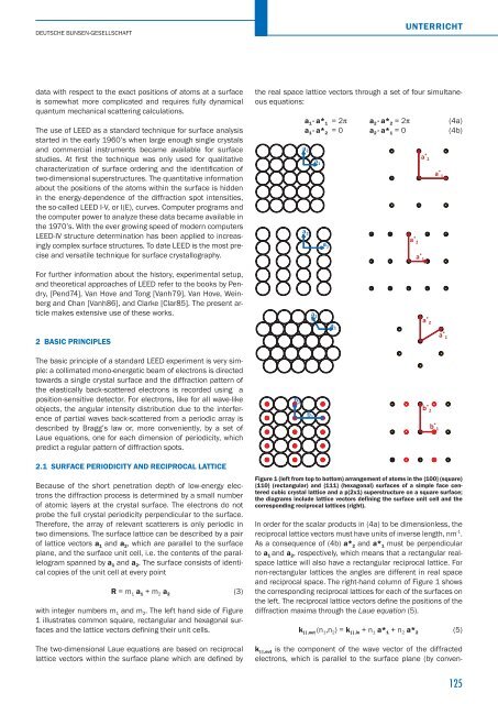
two dimensions. The surface lattice can be described by a pair<br />
of lattice vectors a 1 and a 2, which are parallel to the surface<br />
plane, and the surface unit cell, i.e. the contents of the parallelogram<br />
spanned by a 1 and a 2. The surface consists of identical<br />
copies of the unit cell at every point<br />
R = m 1 a 1 + m 2 a 2<br />
with integer numbers m 1 and m 2. The left hand side of Figure<br />
1 illustrates common square, rectangular and hexagonal surfaces<br />
and the lattice vectors defi ning their unit cells.<br />
The two-dimensional Laue equations are based on reciprocal<br />
lattice vectors within the surface plane which are defi ned by<br />
(3)<br />
UNTERRICHT<br />
the real space lattice vectors through a set of four simultaneous<br />
equations:<br />
b 2<br />
a 1 ∙ a* 1 = 2p a 2 ∙ a* 2 = 2p (4a)<br />
a 1 ∙ a* 2 = 0 a 2 ∙ a* 1 = 0 (4b)<br />
a 2<br />
a 2<br />
b 1<br />
a 2<br />
a 1<br />
a 1<br />
a 1<br />
Figure 1 (left from top to bottom) arrangement of atoms in the {100} (square)<br />
{110} (rectangular) and {111} (hexagonal) surfaces of a simple face centered<br />
cubic crystal lattice and a p(2x1) superstructure on a square surface;<br />
the diagrams include lattice vectors defining the surface unit cell and the<br />
corresponding reciprocal lattices (right).<br />
In order for the scalar products in (4a) to be dimensionless, the<br />
reciprocal lattice vectors must have units of inverse length, nm -1 .<br />
As a consequence of (4b) a* 2 and a* 1 must be perpendicular<br />
to a 1 and a 2, respectively, which means that a rectangular realspace<br />
lattice will also have a rectangular reciprocal lattice. For<br />
non-rectangular lattices the angles are different in real space<br />
and reciprocal space. The right-hand column of Figure 1 shows<br />
the corresponding reciprocal lattices for each of the surfaces on<br />
the left. The reciprocal lattice vectors defi ne the positions of the<br />
diffraction maxima through the Laue equation (5).<br />
a * 2<br />
k ||,out (n 1,n 2) = k ||,in + n 1 a* 1 + n 2 a* 2<br />
k ||,out is the component of the wave vector of the diffracted<br />
electrons, which is parallel to the surface plane (by conven-<br />
a * 1<br />
a * 2<br />
a * 2<br />
b * 2<br />
b * 1<br />
a * 1<br />
a * 1<br />
(5)<br />
125