Electro Optical Characterisation of Short Wavelength Semiconductor ...
Electro Optical Characterisation of Short Wavelength Semiconductor ...
Electro Optical Characterisation of Short Wavelength Semiconductor ...

Create successful ePaper yourself
Turn your PDF publications into a flip-book with our unique Google optimized e-Paper software.
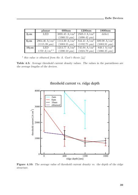
planar 600nm 1200nm 1800nm<br />
2µm LED 3895.45 A/cm 2 2505.3 A/cm 2 defect<br />
(1360.53 µm) (1098.42 µm)<br />
6µm 2864.46 A/cm 2 1113.30 A/cm 2 844.41 A/cm 2 689.98 A/cm 2<br />
(1115.39 µm) (1083.55 µm) (1192.75 µm) (1083.91 µm)<br />
10µm LED 1213.77 A/cm 2 745.94 A/cm 2 849.1 A/cm 2<br />
1370 A/cm 2 † (1390.10 µm) (1024.79 µm) (1066.35 µm)<br />
† this value is obtained from the A. Gust’s thesis [44]<br />
ZnSe Devices<br />
Table 4.5: Average threshold current density values. The values in the parentheses are<br />
the average lengths <strong>of</strong> the devices.<br />
threshold current [A/cm 2 ]<br />
4000<br />
3000<br />
2000<br />
1000<br />
0<br />
threshold current vs. ridge depth<br />
2um<br />
6um<br />
10um<br />
obtained<br />
0 600 1200 1800<br />
ridge depth [nm]<br />
Figure 4.10: The average value <strong>of</strong> threshold current density vs. the depth <strong>of</strong> the ridge<br />
structure.<br />
39