Electro Optical Characterisation of Short Wavelength Semiconductor ...
Electro Optical Characterisation of Short Wavelength Semiconductor ...
Electro Optical Characterisation of Short Wavelength Semiconductor ...

Create successful ePaper yourself
Turn your PDF publications into a flip-book with our unique Google optimized e-Paper software.
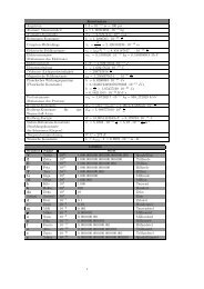
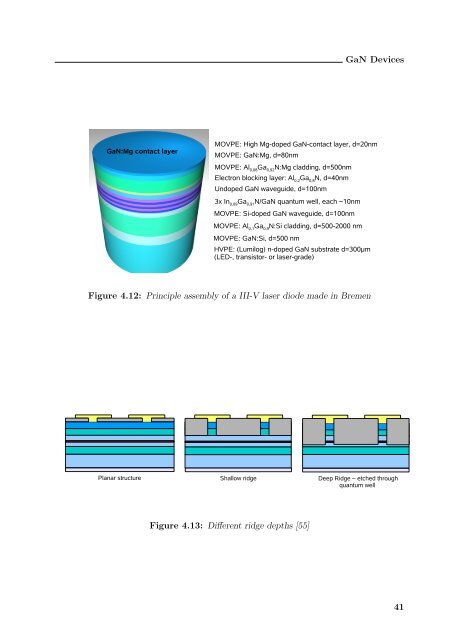
GaN:Mg contact layer<br />
GaN Devices<br />
MOVPE: High Mg-doped GaN-contact layer, d=20nm<br />
MOVPE: GaN:Mg, d=80nm<br />
MOVPE: Al 0,08 Ga 0,92 N:Mg cladding, d=500nm<br />
<strong>Electro</strong>n blocking layer: Al 0,2 Ga 0,8 N, d=40nm<br />
Undoped GaN waveguide, d=100nm<br />
3x In 0,09 Ga 0,91 N/GaN quantum well, each ~10nm<br />
MOVPE: Si-doped GaN waveguide, d=100nm<br />
MOVPE: Al 0,1 Ga 0,9 N:Si cladding, d=500-2000 nm<br />
MOVPE: GaN:Si, d=500 nm<br />
HVPE: (Lumilog) n-doped GaN substrate d=300µm<br />
(LED-, transistor- or laser-grade)<br />
Figure 4.12: Principle assembly <strong>of</strong> a III-V laser diode made in Bremen<br />
Planar structure Shallow ridge Deep Ridge – etched through<br />
quantum well<br />
Figure 4.13: Different ridge depths [55]<br />
41