LOGIC DESIGN LABORATORY MANUAL - VTU e-Learning Centre
LOGIC DESIGN LABORATORY MANUAL - VTU e-Learning Centre
LOGIC DESIGN LABORATORY MANUAL - VTU e-Learning Centre

Create successful ePaper yourself
Turn your PDF publications into a flip-book with our unique Google optimized e-Paper software.
Logic Design Laboratory Manual 39<br />
___________________________________________________________________________<br />
EXPERIMENT: 12<br />
FLIP FLOPS<br />
AIM: Truth Table verification of<br />
1) RS Flip Flop<br />
2) T type Flip Flop.<br />
3) D type Flip Flop.<br />
4) JK Flip Flop.<br />
5) JK Master Slave Flip Flop.<br />
LEARNING OBJECTIVE:<br />
To learn about various Flip-Flops<br />
To learn and understand the working of Master slave FF<br />
To learn about applications of FFs<br />
Conversion of one type of Flip flop to another<br />
COMPONENTS REQUIRED:<br />
IC 7408, IC 7404, IC 7402, IC 7400, Patch Cords & IC Trainer Kit.<br />
THEORY:<br />
Logic circuits that incorporate memory cells are called sequential logic circuits; their output<br />
depends not only upon the present value of the input but also upon the previous values.<br />
Sequential logic circuits often require a timing generator (a clock) for their operation.<br />
The latch (flip-flop) is a basic bi-stable memory element widely used in sequential logic<br />
circuits. Usually there are two outputs, Q and its complementary value.<br />
Some of the most widely used latches are listed below.<br />
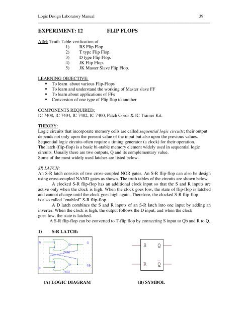
SR LATCH:<br />
An S-R latch consists of two cross-coupled NOR gates. An S-R flip-flop can also be design<br />
using cross-coupled NAND gates as shown. The truth tables of the circuits are shown below.<br />
A clocked S-R flip-flop has an additional clock input so that the S and R inputs are<br />
active only when the clock is high. When the clock goes low, the state of flip-flop is latched<br />
and cannot change until the clock goes high again. Therefore, the clocked S-R flip-flop<br />
is also called “enabled” S-R flip-flop.<br />
A D latch combines the S and R inputs of an S-R latch into one input by adding an<br />
inverter. When the clock is high, the output follows the D input, and when the clock<br />
goes low, the state is latched.<br />
A S-R flip-flop can be converted to T-flip flop by connecting S input to Qb and R to Q.<br />
1) S-R LATCH:<br />
(A) <strong>LOGIC</strong> DIAGRAM<br />
(B) SYMBOL