LOGIC DESIGN LABORATORY MANUAL - VTU e-Learning Centre
LOGIC DESIGN LABORATORY MANUAL - VTU e-Learning Centre
LOGIC DESIGN LABORATORY MANUAL - VTU e-Learning Centre

You also want an ePaper? Increase the reach of your titles
YUMPU automatically turns print PDFs into web optimized ePapers that Google loves.
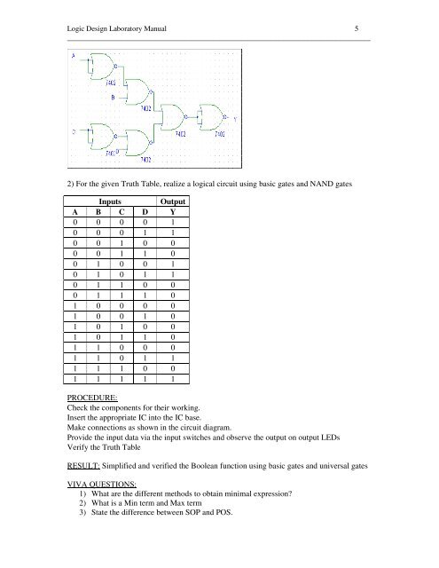
Logic Design Laboratory Manual 5<br />
___________________________________________________________________________<br />
2) For the given Truth Table, realize a logical circuit using basic gates and NAND gates<br />
Inputs Output<br />
A B C D Y<br />
0 0 0 0 1<br />
0 0 0 1 1<br />
0 0 1 0 0<br />
0 0 1 1 0<br />
0 1 0 0 1<br />
0 1 0 1 1<br />
0 1 1 0 0<br />
0 1 1 1 0<br />
1 0 0 0 0<br />
1 0 0 1 0<br />
1 0 1 0 0<br />
1 0 1 1 0<br />
1 1 0 0 0<br />
1 1 0 1 1<br />
1 1 1 0 0<br />
1 1 1 1 1<br />
PROCEDURE:<br />
Check the components for their working.<br />
Insert the appropriate IC into the IC base.<br />
Make connections as shown in the circuit diagram.<br />
Provide the input data via the input switches and observe the output on output LEDs<br />
Verify the Truth Table<br />
RESULT: Simplified and verified the Boolean function using basic gates and universal gates<br />
VIVA QUESTIONS:<br />
1) What are the different methods to obtain minimal expression?<br />
2) What is a Min term and Max term<br />
3) State the difference between SOP and POS.