Burn-in & Test Socket Workshop - BiTS Workshop
Burn-in & Test Socket Workshop - BiTS Workshop
Burn-in & Test Socket Workshop - BiTS Workshop

Create successful ePaper yourself
Turn your PDF publications into a flip-book with our unique Google optimized e-Paper software.
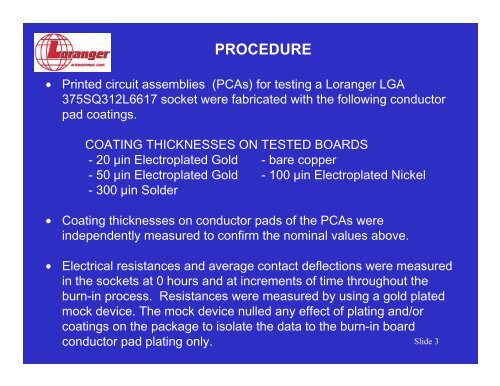
PROCEDURE<br />
• Pr<strong>in</strong>ted circuit assemblies (PCAs) for test<strong>in</strong>g a Loranger LGA<br />
375SQ312L6617 socket were fabricated with the follow<strong>in</strong>g conductor<br />
pad coat<strong>in</strong>gs.<br />
COATING THICKNESSES ON TESTED BOARDS<br />
- 20 µ<strong>in</strong> Electroplated Gold - bare copper<br />
- 50 µ<strong>in</strong> Electroplated Gold - 100 µ<strong>in</strong> Electroplated Nickel<br />
- 300 µ<strong>in</strong> Solder<br />
• Coat<strong>in</strong>g thicknesses on conductor pads of the PCAs were<br />
<strong>in</strong>dependently measured to confirm the nom<strong>in</strong>al values above.<br />
• Electrical resistances and average contact deflections were measured<br />
<strong>in</strong> the sockets at 0 hours and at <strong>in</strong>crements of time throughout the<br />
burn-<strong>in</strong> process. Resistances were measured by us<strong>in</strong>g a gold plated<br />
mock device. The mock device nulled any effect of plat<strong>in</strong>g and/or<br />
coat<strong>in</strong>gs on the package to isolate the data to the burn-<strong>in</strong> board<br />
conductor pad plat<strong>in</strong>g only.<br />
Slide 3