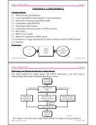
Create successful ePaper yourself
Turn your PDF publications into a flip-book with our unique Google optimized e-Paper software.
Chapter 6 – Section 2 (5/2/04) Page 6.2-16<br />
Summary of the Conditions for Stability of the Two-Stage Op Amp<br />
• Unity-gainbandwith is given as:<br />
⎛ 1 ⎞<br />
⎜<br />
⎟<br />
GB = A v (0)·|p 1 | = (g mI g mII R I R II g ⎟<br />
)·⎝⎜ mII R I R II C c<br />
= g mI<br />
⎛ 1 ⎞<br />
⎜<br />
⎟<br />
⎠<br />
C c<br />
= (g m1 g m2 R 1 R 2 g ⎟<br />
)·⎝⎜ m2 R 1 R 2 C c<br />
= g m1<br />
⎠<br />
C c<br />
• The requirement for 45° phase margin is:<br />
⎛ ω ⎞<br />
±180° - Arg[AF] = ±180° - tan-1⎜<br />
⎟<br />
⎝ |p1| - tan ⎛ ω ⎞<br />
-1⎜<br />
⎟<br />
⎠<br />
⎝ |p2| - tan ⎛ω⎞<br />
-1⎜<br />
⎟<br />
⎠<br />
⎝ z = 45° ⎠<br />
Let ω = GB and assume that z ≥ 10GB, therefore we get,<br />
⎛GB⎞<br />
±180° - tan-1⎜<br />
⎟<br />
⎝ |p1| - tan ⎛GB⎞<br />
-1⎜<br />
⎟<br />
⎠<br />
⎝ |p2| - tan ⎛GB⎞<br />
-1⎜<br />
⎟<br />
⎠<br />
⎝ z = 45° ⎠<br />
⎛GB⎞<br />
135° ≈ tan-1(Av(0)) + tan-1⎜<br />
⎟<br />
⎝ |p2| + tan ⎛GB⎞<br />
-1(0.1) = 90° + tan-1⎜<br />
⎟<br />
⎠<br />
⎝ |p2| + 5.7°<br />
⎠<br />
⎛GB⎞<br />
39.3° ≈ tan-1⎜<br />
⎟<br />
⎝ |p2| ⇒ GB<br />
⎠ |p 2 | = 0.818 ⇒ |p 2| ≥ 1.22GB<br />
• The requirement for 60° phase margin:<br />
|p2| ≥ 2.2GB if z ≥ 10GB<br />
• If 60° phase margin is required, then the following relationships apply:<br />
gm6<br />
Cc > 10g m1<br />
Cc ⇒ g m6 > 10gm1 and g m6<br />
C2 > 2.2g m1<br />
Cc ⇒ Cc > 0.22C2<br />
CMOS <strong>Analog</strong> Circuit <strong>Design</strong> © P.E. Allen - 2004<br />
Chapter 6 – Section 2 (5/2/04) Page 6.2-17<br />
Controlling the Right-Half Plane Zero<br />
Why is the RHP zero a problem?<br />
Because it boosts the magnitude but lags the phase - the worst possible combination for<br />
stability.<br />
jω<br />
jω 3<br />
θ1 θ 2<br />
jω 2<br />
180° > θ 1 > θ 2 > θ 3<br />
jω 1<br />
θ3<br />
σ<br />
Fig. 430-01<br />
Solution of the problem:<br />
If a zero is caused by two paths to the output, then eliminate one of the paths.<br />
z 1<br />
CMOS <strong>Analog</strong> Circuit <strong>Design</strong> © P.E. Allen - 2004