You also want an ePaper? Increase the reach of your titles
YUMPU automatically turns print PDFs into web optimized ePapers that Google loves.
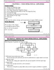
Chapter 6 – Section 1 (5/2/04) Page 6.1-2<br />
Ideal Op Amp<br />
Symbol:<br />
i 1<br />
V DD<br />
+<br />
+ +<br />
i 2<br />
v -<br />
v i<br />
1 -<br />
+<br />
+<br />
v OUT = A v (v 1 -v 2 )<br />
v 2<br />
-<br />
-<br />
V SS<br />
-<br />
Fig. 110-02<br />
Null port:<br />
If the differential gain of the op amp is large enough then input terminal pair becomes a<br />
null port.<br />
A null port is a pair of terminals where the voltage is zero and the current is zero.<br />
I.e.,<br />
v 1 - v 2 = v i = 0<br />
and<br />
i 1 = 0 and i 2 = 0<br />
Therefore, ideal op amps can be analyzed by assuming the differential input voltage is<br />
zero and that no current flows into or out of the differential inputs.<br />
CMOS <strong>Analog</strong> Circuit <strong>Design</strong> © P.E. Allen - 2004<br />
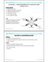
Chapter 6 – Section 1 (5/2/04) Page 6.1-3<br />
General Configuration of the Op Amp as a Voltage Amplifier<br />
R 1<br />
- R2<br />
+ +<br />
v<br />
+<br />
inn<br />
v inp<br />
v 2<br />
v 1<br />
- -<br />
Noniverting voltage amplifier:<br />
⎛R ⎜ 1 +R 2<br />
⎞<br />
⎟<br />
v inn = 0 ⇒ v out = ⎜ ⎟<br />
⎝<br />
R 1<br />
v<br />
⎠ inp<br />
Inverting voltage amplifier:<br />
v inp = 0 ⇒ v out = - R ⎜⎛ 2<br />
⎜ ⎝<br />
R 1 ⎠ ⎟⎟⎞ v inn<br />
+<br />
vout<br />
-<br />
Fig. 110-03<br />
CMOS <strong>Analog</strong> Circuit <strong>Design</strong> © P.E. Allen - 2004