
Create successful ePaper yourself
Turn your PDF publications into a flip-book with our unique Google optimized e-Paper software.
Chapter 6 – Introduction (5/2/04) Page 6.0-1<br />
CHAPTER 6 – CMOS OPERATIONAL AMPLIFIERS<br />
Chapter Outline<br />
6.1 <strong>Design</strong> of CMOS Op Amps<br />
6.2 Compensation of Op Amps<br />
6.3 Two-Stage Operational Amplifier <strong>Design</strong><br />
6.4 Power Supply Rejection Ratio of the Two-Stage Op Amp<br />
6.5 Cascode Op Amps<br />
6.6 Simulation and Measurement of Op Amps<br />
6.7 Macromodels for Op Amps<br />
6.8 Summary<br />
Goal<br />
Understand the analysis, design, and measurement of simple CMOS op amps<br />
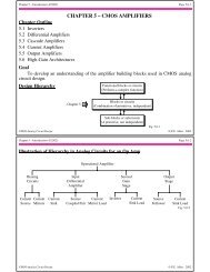
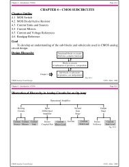
<strong>Design</strong> Hierarchy<br />
The op amps of this <strong>chapter</strong><br />
are unbuffered and are OTAs<br />
but we will use the generic<br />
term “op amp”.<br />
Chapter 6<br />
Functional blocks or circuits<br />
(Perform a complex function)<br />
Blocks or circuits<br />
(Combination of primitives, independent)<br />
Sub-blocks or subcircuits<br />
(A primitive, not independent)<br />
Fig. 6.0-1<br />
CMOS <strong>Analog</strong> Circuit <strong>Design</strong> © P.E. Allen - 2004<br />
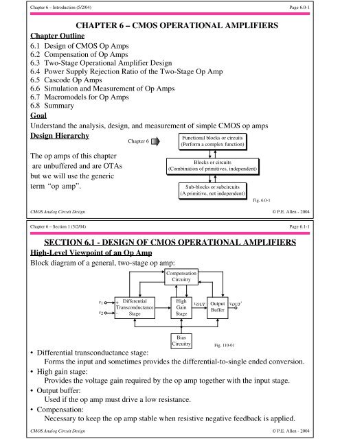
Chapter 6 – Section 1 (5/2/04) Page 6.1-1<br />
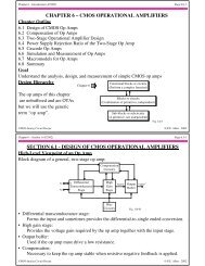
SECTION 6.1 - DESIGN OF CMOS OPERATIONAL AMPLIFIERS<br />
High-Level Viewpoint of an Op Amp<br />
Block diagram of a general, two-stage op amp:<br />
Compensation<br />
Circuitry<br />
v 1<br />
v 2<br />
+ Differential<br />
Transconductance<br />
- Stage<br />
High<br />
Gain<br />
Stage<br />
v OUT<br />
Output<br />
Buffer<br />
v OUT '<br />
Bias<br />
Circuitry<br />
Fig. 110-01<br />
• Differential transconductance stage:<br />
Forms the input and sometimes provides the differential-to-single ended conversion.<br />
• High gain stage:<br />
Provides the voltage gain required by the op amp together with the input stage.<br />
• Output buffer:<br />
Used if the op amp must drive a low resistance.<br />
• Compensation:<br />
Necessary to keep the op amp stable when resistive negative feedback is applied.<br />
CMOS <strong>Analog</strong> Circuit <strong>Design</strong> © P.E. Allen - 2004
Chapter 6 – Section 1 (5/2/04) Page 6.1-2<br />
Ideal Op Amp<br />
Symbol:<br />
i 1<br />
V DD<br />
+<br />
+ +<br />
i 2<br />
v -<br />
v i<br />
1 -<br />
+<br />
+<br />
v OUT = A v (v 1 -v 2 )<br />
v 2<br />
-<br />
-<br />
V SS<br />
-<br />
Fig. 110-02<br />
Null port:<br />
If the differential gain of the op amp is large enough then input terminal pair becomes a<br />
null port.<br />
A null port is a pair of terminals where the voltage is zero and the current is zero.<br />
I.e.,<br />
v 1 - v 2 = v i = 0<br />
and<br />
i 1 = 0 and i 2 = 0<br />
Therefore, ideal op amps can be analyzed by assuming the differential input voltage is<br />
zero and that no current flows into or out of the differential inputs.<br />
CMOS <strong>Analog</strong> Circuit <strong>Design</strong> © P.E. Allen - 2004<br />
Chapter 6 – Section 1 (5/2/04) Page 6.1-3<br />
General Configuration of the Op Amp as a Voltage Amplifier<br />
R 1<br />
- R2<br />
+ +<br />
v<br />
+<br />
inn<br />
v inp<br />
v 2<br />
v 1<br />
- -<br />
Noniverting voltage amplifier:<br />
⎛R ⎜ 1 +R 2<br />
⎞<br />
⎟<br />
v inn = 0 ⇒ v out = ⎜ ⎟<br />
⎝<br />
R 1<br />
v<br />
⎠ inp<br />
Inverting voltage amplifier:<br />
v inp = 0 ⇒ v out = - R ⎜⎛ 2<br />
⎜ ⎝<br />
R 1 ⎠ ⎟⎟⎞ v inn<br />
+<br />
vout<br />
-<br />
Fig. 110-03<br />
CMOS <strong>Analog</strong> Circuit <strong>Design</strong> © P.E. Allen - 2004
Chapter 6 – Section 1 (5/2/04) Page 6.1-4<br />
Example 6.1-1 - Simplified Analysis of an Op Amp Circuit<br />
The circuit shown below is an inverting voltage amplifier using an op amp. Find the<br />
voltage transfer function, v out /v in .<br />
R 1<br />
i 1 i 2<br />
R 2<br />
i i<br />
- + +<br />
+<br />
v in + v i v out<br />
- -<br />
-<br />
Virtual Ground Fig. 110-04<br />
Solution<br />
If A v → ∞, then v i → 0 because of the negative feedback path through R 2 .<br />
(The op amp with –fb. makes its input terminal voltages equal.)<br />
v i = 0 and i i = 0<br />
Note that the null port becomes the familiar virtual ground if one of the op amp input<br />
terminals is on ground. If this is the case, then we can write that<br />
i 1 = v in<br />
R 1<br />
and i 2 = v out<br />
R 2<br />
v out<br />
Since, i i = 0, then i 1 + i 2 = 0 giving the desired result as v in<br />
= - R 2<br />
R 1<br />
.<br />
CMOS <strong>Analog</strong> Circuit <strong>Design</strong> © P.E. Allen - 2004<br />
Chapter 6 – Section 1 (5/2/04) Page 6.1-5<br />
Linear and Static Characterization of the Op Amp<br />
A model for a nonideal op amp that includes some of the linear, static nonidealities:<br />
v 1<br />
CMRR<br />
v 2<br />
v 1<br />
-<br />
+<br />
R icm I B2<br />
e n 2<br />
V OS<br />
*<br />
i n 2 C id R id<br />
R out vout<br />
R icm I B1<br />
Ideal Op Amp<br />
where<br />
R id = differential input resistance<br />
C id = differential input capacitance<br />
R icm = common mode input resistance<br />
V OS = input-offset voltage<br />
I B1 and I B2 = differential input-bias currents<br />
I OS = input-offset current (I OS = I B1 -I B2 )<br />
CMRR = common-mode rejection ratio<br />
e 2 n = voltage-noise spectral density (mean-square volts/Hertz)<br />
i 2 n = current-noise spectral density (mean-square amps/Hertz)<br />
Fig. 110-05<br />
CMOS <strong>Analog</strong> Circuit <strong>Design</strong> © P.E. Allen - 2004
Chapter 6 – Section 1 (5/2/04) Page 6.1-6<br />
Linear and Dynamic Characteristics of the Op Amp<br />
Differential and common-mode frequency response:<br />
⎛V ⎜ 1 (s)+V 2 (s)⎞<br />
⎟<br />
V out (s) = A v (s)[V 1 (s) - V 2 (s)] ± A c (s) ⎜<br />
⎟<br />
⎝ 2 ⎠<br />
Differential-frequency response:<br />
A v0<br />
A v0 p 1 p 2 p 3···<br />
A v (s) =<br />
⎛ s ⎞⎛<br />
s ⎞⎛<br />
s ⎞<br />
= (s -p<br />
⎜ ⎟⎜<br />
⎟⎜<br />
⎟ 1 )(s -p 2 )(s -p 3 )···<br />
⎜ ⎟<br />
⎝p 1<br />
- 1 ⎜ ⎟<br />
⎠⎝p 2<br />
- 1 ⎜ ⎟<br />
⎠⎝p 3<br />
- 1 ···<br />
⎠<br />
where p 1 , p 2 , p 3 ,··· are the poles of the differential-frequency response (ignoring zeros).<br />
20log10(A v0 )<br />
|A v (jω)| dB<br />
Asymptotic<br />
Magnitude<br />
Actual<br />
Magnitude<br />
-6dB/oct.<br />
GB<br />
0dB<br />
Fig. 110-06<br />
ω 1<br />
ω 2 ω 3<br />
ω<br />
-12dB/oct.<br />
-18dB/oct.<br />
CMOS <strong>Analog</strong> Circuit <strong>Design</strong> © P.E. Allen - 2004<br />
Chapter 6 – Section 1 (5/2/04) Page 6.1-7<br />
Other Characteristics of the Op Amp<br />
Power supply rejection ratio (PSRR):<br />
PSRR ∆V DD<br />
= ∆V OUT<br />
A v (s) V o/V in (V dd = 0)<br />
= V o /V dd (V in = 0)<br />
Input common mode range (<strong>IC</strong>MR):<br />
<strong>IC</strong>MR = the voltage range over which the input common-mode signal can vary<br />
without influence the differential performance<br />
Slew rate (SR):<br />
SR = output voltage rate limit of the op amp<br />
Settling time (T s ):<br />
-<br />
+<br />
v OUT<br />
Final Value + ε<br />
Final Value<br />
Final Value - ε<br />
v OUT (t)<br />
ε<br />
ε<br />
Upper Tolerance<br />
Lower Tolerance<br />
Settling Time<br />
0<br />
0<br />
v IN<br />
Fig. 110-07<br />
T s<br />
t<br />
CMOS <strong>Analog</strong> Circuit <strong>Design</strong> © P.E. Allen - 2004
Chapter 6 – Section 1 (5/2/04) Page 6.1-8<br />
Classification of CMOS Op Amps<br />
Categorization of op amps:<br />
Conversion<br />
Hierarchy<br />
Voltage<br />
to Current<br />
Current<br />
to Voltage<br />
Classic Differential<br />
Amplifier<br />
Differential-to-single ended<br />
Load (Current Mirror)<br />
Modified Differential<br />
Amplifier<br />
Source/Sink<br />
Current Loads<br />
MOS Diode<br />
Load<br />
First<br />
Voltage<br />
Stage<br />
Voltage<br />
to Current<br />
Current<br />
to Voltage<br />
Transconductance<br />
Grounded Gate<br />
Class A (Source<br />
or Sink Load)<br />
Transconductance<br />
Grounded Source<br />
Class B<br />
(Push-Pull)<br />
Current<br />
Stage<br />
Second<br />
Voltage<br />
Stage<br />
Table 110-01<br />
CMOS <strong>Analog</strong> Circuit <strong>Design</strong> © P.E. Allen - 2004<br />
Chapter 6 – Section 1 (5/2/04) Page 6.1-9<br />
Two-Stage CMOS Op Amp<br />
Classical two-stage CMOS op amp broken into voltage-to-current and current-to-voltage<br />
stages:<br />
V DD<br />
M3<br />
M4<br />
M6<br />
-<br />
v in<br />
+<br />
M1 M2<br />
v out<br />
v in<br />
-<br />
+<br />
v out<br />
VBias<br />
M5<br />
M7<br />
V→I I→V V→I I→V<br />
V SS<br />
Fig. 6.1-8<br />
CMOS <strong>Analog</strong> Circuit <strong>Design</strong> © P.E. Allen - 2004
Chapter 6 – Section 1 (5/2/04) Page 6.1-10<br />
Folded Cascode CMOS Op Amp<br />
Folded cascode CMOS op amp broken into stages.<br />
V DD<br />
V Bias<br />
M3<br />
M10<br />
M11<br />
+ M1 M2<br />
v -<br />
in M8 M9<br />
v out<br />
-<br />
+<br />
M6 M7<br />
V Bias<br />
v out<br />
v in<br />
Fig. 6.1-9<br />
V Bias<br />
M4 M5<br />
V→I I→I I→V<br />
V SS<br />
CMOS <strong>Analog</strong> Circuit <strong>Design</strong> © P.E. Allen - 2004<br />
Chapter 6 – Section 1 (5/2/04) Page 6.1-11<br />
<strong>Design</strong> of CMOS Op Amps<br />
Steps:<br />
1.) Choosing or creating the basic structure of the op amp.<br />
This step is results in a schematic showing the transistors and their interconnections.<br />
This diagram does not change throughout the remainder of the design unless the<br />
specifications cannot be met, then a new or modified structure must be developed.<br />
2.) Selection of the dc currents and transistor sizes.<br />
Most of the effort of design is in this category.<br />
Simulators are used to aid the designer in this phase. The general performance of the<br />
circuit should be known a priori.<br />
3.) Physical implementation of the design.<br />
Layout of the transistors<br />
Floorplanning the connections, pin-outs, power supply buses and grounds<br />
Extraction of the physical parasitics and resimulation<br />
Verification that the layout is a physical representation of the circuit.<br />
4.) Fabrication<br />
5.) Measurement<br />
Verification of the specifications<br />
Modification of the design as necessary<br />
CMOS <strong>Analog</strong> Circuit <strong>Design</strong> © P.E. Allen - 2004
Chapter 6 – Section 1 (5/2/04) Page 6.1-12<br />
Boundary Conditions and Requirements for CMOS Op Amps<br />
Boundary conditions:<br />
1. Process specification (V T , K', C ox , etc.)<br />
2. Supply voltage and range<br />
3. Supply current and range<br />
4. Operating temperature and range<br />
Requirements:<br />
1. Gain<br />
2. Gain bandwidth<br />
3. Settling time<br />
4. Slew rate<br />
5. Common-mode input range, <strong>IC</strong>MR<br />
6. Common-mode rejection ratio, CMRR<br />
7. Power-supply rejection ratio, PSRR<br />
8. Output-voltage swing<br />
9. Output resistance<br />
10. Offset<br />
11. Noise<br />
12. Layout area<br />
CMOS <strong>Analog</strong> Circuit <strong>Design</strong> © P.E. Allen - 2004<br />
Chapter 6 – Section 1 (5/2/04) Page 6.1-13<br />
Specifications for a Typical Unbuffered CMOS Op Amp<br />
Boundary Conditions Requirement<br />
Process Specification See Tables 3.1-1 and 3.1-2<br />
Supply Voltage ±2.5 V ±10%<br />
Supply Current 100 µA<br />
Temperature Range 0 to 70°C<br />
Specifications<br />
Value<br />
Gain<br />
≥ 70 dB<br />
Gainbandwidth ≥ 5 MHz<br />
Settling Time<br />
≤ 1 µsec<br />
Slew Rate<br />
≥ 5 V/µsec<br />
Input CMR<br />
≥ ±1.5 V<br />
CMRR<br />
≥ 60 dB<br />
PSRR<br />
≥ 60 dB<br />
Output Swing<br />
≥ ±1.5 V<br />
Output Resistance N/A, capacitive load only<br />
Offset<br />
≤ ±10 mV<br />
Noise<br />
≤ 100nV/ Hz at 1KHz<br />
Layout Area ≤ 10,000 min. channel length 2<br />
CMOS <strong>Analog</strong> Circuit <strong>Design</strong> © P.E. Allen - 2004
Chapter 6 – Section 1 (5/2/04) Page 6.1-14<br />
Some Practical Thoughts on Op Amp <strong>Design</strong><br />
1.) Decide upon a suitable topology.<br />
• Experience is a great help<br />
• The topology should be the one capable of meeting most of the specifications<br />
• Try to avoid “inventing” a new topology but start with an existing topology<br />
2.) Determine the type of compensation needed to meet the specifications.<br />
• Consider the load and stability requirements<br />
• Use some form of Miller compensation or a self-compensated approach (shown<br />
later)<br />
3.) <strong>Design</strong> dc currents and device sizes for proper dc, ac, and transient performance.<br />
• This begins with hand calculations based upon approximate design equations.<br />
• Compensation components are also sized in this step of the procedure.<br />
• After each device is sized by hand, a circuit simulator is used to fine tune the design<br />
Two basic steps of design:<br />
1.) “First-cut” - this step is to use hand calculations to propose a design that has<br />
potential of satisfying the specifications. <strong>Design</strong> robustness is developed in this step.<br />
2.) Optimization - this step uses the computer to refine and optimize the design.<br />
CMOS <strong>Analog</strong> Circuit <strong>Design</strong> © P.E. Allen - 2004<br />
Chapter 6 – Section 2 (5/2/04) Page 6.2-1<br />
SECTION 6.2 - COMPENSATION OF OP AMPS<br />
Compensation<br />
Objective<br />
Objective of compensation is to achieve stable operation when negative feedback is<br />
applied around the op amp.<br />
Types of Compensation<br />
1. Miller - Use of a capacitor feeding back around a high-gain, inverting<br />
stage.<br />
• Miller capacitor only<br />
• Miller capacitor with an unity-gain buffer to block the forward path through the<br />
compensation capacitor. Can eliminate the RHP zero.<br />
• Miller with a nulling resistor. Similar to Miller but with an added series resistance<br />
to gain control over the RHP zero.<br />
2. Self compensating - Load capacitor compensates the op amp (later).<br />
3. Feedforward - Bypassing a positive gain amplifier resulting in phase lead. Gain can be<br />
less than unity.<br />
CMOS <strong>Analog</strong> Circuit <strong>Design</strong> © P.E. Allen - 2004
Chapter 6 – Section 2 (5/2/04) Page 6.2-2<br />
Single-Loop, Negative Feedback Systems<br />
Block diagram:<br />
A(s) = differential-mode voltage gain of the<br />
op amp<br />
F(s) = feedback transfer function from the<br />
output of op amp back to the input.<br />
Definitions:<br />
• Open-loop gain = L(s) = -A(s)F(s)<br />
• Closed-loop gain = V out(s)<br />
V in (s) = A(s)<br />
1+A(s)F(s)<br />
V in (s)<br />
Stability Requirements:<br />
The requirements for stability for a single-loop, negative feedback system is,<br />
|A(jω 0° )F(jω 0° )| = |L(jω 0° )| < 1<br />
where ω 0° is defined as<br />
Arg[−A(jω 0° )F(jω 0° )] = Arg[L(jω 0° )] = 0°<br />
Another convenient way to express this requirement is<br />
Arg[−A(jω 0dB )F(jω 0dB )] = Arg[L(jω 0dB )] > 0°<br />
where ω 0dB is defined as<br />
|A(jω 0dB )F(jω 0dB )| = |L(jω 0dB )| = 1<br />
+<br />
-<br />
Σ<br />
F(s)<br />
A(s)<br />
V out (s)<br />
Fig. 120-01<br />
CMOS <strong>Analog</strong> Circuit <strong>Design</strong> © P.E. Allen - 2004<br />
Chapter 6 – Section 2 (5/2/04) Page 6.2-3<br />
Illustration of the Stability Requirement using Bode Plots<br />
|A(jω)F(jω)|<br />
Arg[-A(jω)F(jω)]<br />
0dB<br />
180°<br />
135°<br />
90°<br />
45°<br />
0°<br />
-20dB/decade<br />
ω 0dB<br />
ω<br />
-40dB/decade<br />
Frequency (rads/sec.)<br />
A measure of stability is given by the phase when |A(jω)F(jω)| = 1. This phase is called<br />
phase margin.<br />
Phase margin = Φ M = Arg[-A(jω 0dB )F(jω 0dB )] = Arg[L(jω 0dB )]<br />
Φ M<br />
ω<br />
Fig. Fig. 120-02<br />
CMOS <strong>Analog</strong> Circuit <strong>Design</strong> © P.E. Allen - 2004
Chapter 6 – Section 2 (5/2/04) Page 6.2-4<br />
Why Do We Want Good Stability?<br />
Consider the step response of second-order system which closely models the closed-loop<br />
gain of the op amp.<br />
v out (t)<br />
A v0<br />
1.4<br />
1.2<br />
1.0<br />
0.8<br />
0.6<br />
0.4<br />
45°<br />
50°<br />
55°<br />
60°<br />
65°<br />
70°<br />
-<br />
+<br />
0.2<br />
0<br />
0 5 10 15 Fig. 120-03<br />
ω o t = ω n t (sec.)<br />
A “good” step response is one that quickly reaches its final value.<br />
Therefore, we see that phase margin should be at least 45° and preferably 60° or larger.<br />
(A rule of thumb for satisfactory stability is that there should be less than three rings.)<br />
Note that good stability is not necessarily the quickest risetime.<br />
CMOS <strong>Analog</strong> Circuit <strong>Design</strong> © P.E. Allen - 2004<br />
Chapter 6 – Section 2 (5/2/04) Page 6.2-5<br />
Uncompensated Frequency Response of Two-Stage Op Amps<br />
Two-Stage Op Amps:<br />
V DD<br />
V CC<br />
M3<br />
M4<br />
M6<br />
Q3<br />
Q4<br />
Q6<br />
-<br />
v in<br />
+<br />
M1 M2<br />
v out<br />
-<br />
v in<br />
Q1 Q2<br />
+<br />
v out<br />
+<br />
VBias<br />
-<br />
Small-Signal Model:<br />
M5<br />
V SS<br />
M7<br />
+<br />
VBias<br />
-<br />
Q5<br />
V EE<br />
Q7<br />
Fig. 120-04<br />
g m1 v in<br />
2<br />
D1, D3 (C1, C3) D2, D4 (C2, C4) D6, D7 (C6, C7)<br />
+<br />
R 1 C 1 v1 g +<br />
+<br />
m2v in<br />
v out<br />
2<br />
-<br />
g m4 v 1<br />
R 2 C<br />
v2 R 3 C 3 2 - gm6 v 2<br />
-<br />
Fig. 120-05<br />
Note that this model neglects the base-collector and gate-drain capacitances for purposes<br />
of simplification.<br />
CMOS <strong>Analog</strong> Circuit <strong>Design</strong> © P.E. Allen - 2004
Chapter 6 – Section 2 (5/2/04) Page 6.2-6<br />
Uncompensated Frequency Response of Two-Stage Op Amps - Continued<br />
For the MOS two-stage op amp:<br />
1<br />
1<br />
R 1 ≈ g ||r m3 ds3 ||r ds1 ≈ g R m3 2 = r ds2 || r ds4 and R 3 = r ds6 || r ds7<br />
C 1 = C gs3 +C gs4 +C bd1 +C bd3 C 2 = C gs6 +C bd2 +C bd4 and C 3 = C L +C bd6 +C bd7<br />
For the BJT two-stage op amp:<br />
1<br />
R 1 = g m3<br />
||r π3 ||r π4 ||r o1 ||r o3 ≈ 1<br />
g m3<br />
R 2 = r π6 || r o2 || r o4 ≈ r π6 and R 3 = r o6 || r o7<br />
C 1 = C π3 +C π4 +C cs1 +C cs3 C 2 = C π6 +C cs2 +C cs4 and C 3 = C L +C cs6 +C cs7<br />
Assuming the pole due to C 1 is much greater than the poles due to C 2 and C 3 gives,<br />
+<br />
+<br />
g m1 v in v out<br />
R 2 C<br />
v2 R 3 C 3 2 - gm6 v 2<br />
-<br />
+<br />
+<br />
g m1 V in V V out<br />
R I C I R II C II I - gmII V I<br />
-<br />
Fig. 120-06<br />
The locations for the two poles are given by the following equations<br />
p’ 1 = −1<br />
−1<br />
R I C I<br />
and p’ 2 = R II C II<br />
where R I (R II ) is the resistance to ground seen from the output of the first (second) stage<br />
and C I (C II ) is the capacitance to ground seen from the output of the first (second) stage.<br />
CMOS <strong>Analog</strong> Circuit <strong>Design</strong> © P.E. Allen - 2004<br />
Chapter 6 – Section 2 (5/2/04) Page 6.2-7<br />
Uncompensated Frequency Response of an Op Amp<br />
A vd (0) dB<br />
-20dB/decade<br />
|A(jω)|<br />
Arg[-A(jω)]<br />
0dB<br />
Phase Shift<br />
180°<br />
135°<br />
90°<br />
45°<br />
0°<br />
-45°/decade<br />
|p 1 '|<br />
log 10 (ω)<br />
CMOS <strong>Analog</strong> Circuit <strong>Design</strong> © P.E. Allen - 2004<br />
GB<br />
-45°/decade<br />
-40dB/decade<br />
log 10 (ω)<br />
|p 2 '| ω 0dB Fig. 120-07<br />
If we assume that F(s) = 1 (this is the worst case for stability considerations), then the<br />
above plot is the same as the loop gain.<br />
Note that the phase margin is much less than 45°.<br />
Therefore, the op amp must be compensated before using it in a closed-loop<br />
configuration.
Chapter 6 – Section 2 (5/2/04) Page 6.2-8<br />
Miller Compensation of the Two-Stage Op Amp<br />
V DD<br />
V CC<br />
M3<br />
M1<br />
-<br />
M2<br />
v in<br />
+<br />
+<br />
VBias<br />
-<br />
C M<br />
M5<br />
M4<br />
V SS<br />
Q3 Q4<br />
M6<br />
C M<br />
Q6<br />
C c v out<br />
C c v out<br />
-<br />
Q1 Q2<br />
C<br />
v I<br />
C II in C<br />
+<br />
I<br />
C II<br />
M7<br />
+<br />
VBias<br />
-<br />
The various capacitors are:<br />
C c = accomplishes the Miller compensation<br />
C M = capacitance associated with the first-stage mirror (mirror pole)<br />
C I = output capacitance to ground of the first-stage<br />
C II = output capacitance to ground of the second-stage<br />
Q5<br />
V EE<br />
Q7<br />
Fig. 120-08<br />
CMOS <strong>Analog</strong> Circuit <strong>Design</strong> © P.E. Allen - 2004<br />
Chapter 6 – Section 2 (5/2/04) Page 6.2-9<br />
Compensated Two-Stage, Small-Signal Frequency Response Model Simplified<br />
Use the CMOS op amp to illustrate:<br />
1.) Assume that g m3 >> g ds3 + g ds1<br />
2.) Assume that g m3<br />
C M<br />
>> GB<br />
Therefore,<br />
v 1 v2<br />
C c<br />
+<br />
-g m1 v in<br />
2 1 g m2 v in<br />
C M g m3 2 g m4 v 1<br />
C 1 rds2 ||r ds4<br />
g m6 v 2 r ds6 ||r ds7 C L<br />
v out<br />
-<br />
r ds1 ||r ds3<br />
g m1 v in rds2 ||r ds4<br />
g m6 v 2 rds6 ||r ds7<br />
C II<br />
+<br />
v in<br />
-<br />
CI<br />
C c<br />
v 2<br />
+<br />
v out<br />
-<br />
Fig. 120-09<br />
Same circuit holds for the BJT op amp with different component relationships.<br />
CMOS <strong>Analog</strong> Circuit <strong>Design</strong> © P.E. Allen - 2004
Chapter 6 – Section 2 (5/2/04) Page 6.2-10<br />
General Two-Stage Frequency Response Analysis<br />
+<br />
V in<br />
-<br />
g mI V in<br />
C I RI gmII V 2<br />
R II C II<br />
where<br />
g mI = g m1 = gm2, R I = r ds2 ||r ds4 , C I = C 1<br />
and<br />
g mII = g m6 , R II = r ds6 ||r ds7 , C II = C 2 = C L<br />
Nodal Equations:<br />
-g mI V in = [G I + s(C I + C c )]V 2 - [sC c ]V out and 0 = [g mII - sC c ]V 2 + [G II + sC II + sC c ]V out<br />
Solving using Cramer’s rule gives,<br />
V out (s)<br />
V in (s) = g mI (g mII - sC c )<br />
G I G II +s [G II (C I +C II )+G I (C II +C c )+g mII C c ]+s 2 [C I C II +C c C I +C c C II ]<br />
A o [1 - s (C c /g mII )]<br />
= 1+s [R I (C I +C II )+R II (C 2 +C c )+g mII R 1 R II C c ]+s 2 [R I R II (C I C II +C c C I +C c C II )]<br />
where, A o = g mI g mII R I R II<br />
⎛ ⎞<br />
⎜ ⎟<br />
In general, D(s) = ⎜1- s p ⎟ ⎜ ⎜ ⎛<br />
1 ⎝ ⎠ ⎟ ⎟<br />
1- s ⎞ ⎛ 1 ⎞<br />
⎜ ⎟<br />
p = 1-s ⎜ ⎟<br />
2 p + 1<br />
1 p + s2<br />
2 p 1 p → D(s) ≈ 1- s<br />
2<br />
p + s2<br />
1 p 1 p , if |p 2 |>>|p 1 |<br />
2<br />
∴ p 1 =<br />
V 2<br />
C c<br />
+<br />
⎝<br />
⎠<br />
⎝<br />
V out<br />
-<br />
Fig.120-10<br />
-1<br />
-1<br />
R I (C I +C II )+R II (C II +C c )+g mII R 1 R II C c<br />
≈ g mII R 1 R II C c<br />
, z = g mII<br />
C c<br />
⎠<br />
p 2 = -[R I(C I +C II )+R II (C II +C c )+g mII R 1 R II C c ] -g mII C c<br />
R I R II (C I C II +C c C I +C c C II ) ≈ C I C II +C c C I +C c C II<br />
≈ -g mII<br />
C II<br />
, C II > C c > C I<br />
CMOS <strong>Analog</strong> Circuit <strong>Design</strong> © P.E. Allen - 2004<br />
Chapter 6 – Section 2 (5/2/04) Page 6.2-11<br />
Summary of Results for Miller Compensation of the Two-Stage Op Amp<br />
There are three roots of importance:<br />
1.) Right-half plane zero:<br />
z 1 = g mII<br />
C c<br />
= g m6<br />
C c<br />
This root is very undesirable- it boosts the magnitude while decreasing the phase.<br />
2.) Dominant left-half plane pole (the Miller pole):<br />
-1<br />
p 1 ≈ g mII R I R II C c<br />
= -(g ds2+g ds4 )(g ds6 +g ds7 )<br />
g m6 C c<br />
This root accomplishes the desired compensation.<br />
3.) Left-half plane output pole:<br />
p 2 ≈ -g mII<br />
C II<br />
≈ -g m6<br />
C L<br />
This pole must be ≥ unity-gainbandwidth or the phase margin will not be satisfied.<br />
Root locus plot of the Miller compensation:<br />
Closed-loop poles, C c ≠0<br />
Open-loop poles<br />
C c =0<br />
jω<br />
σ<br />
p 2 p 2 ' p 1 ' p 1<br />
z 1 Fig. 120-11<br />
CMOS <strong>Analog</strong> Circuit <strong>Design</strong> © P.E. Allen - 2004
Chapter 6 – Section 2 (5/2/04) Page 6.2-12<br />
Compensated Open-Loop Frequency Response of the Two-Stage Op Amp<br />
|A(jω)F(jω)|<br />
A vd (0) dB<br />
Compensated<br />
Uncompensated<br />
-20dB/decade<br />
Arg[-A(jω)F(jω)|<br />
Note that the unity-gainbandwidth, GB, is<br />
GB<br />
0dB<br />
log 10 (ω)<br />
Phase Shift<br />
Uncompensated<br />
-40dB/decade<br />
180°<br />
135°<br />
-45°/decade<br />
90°<br />
-45°/decade<br />
Compensated<br />
45°<br />
Phase<br />
No phase margin<br />
Margin<br />
0°<br />
log 10 (ω)<br />
|p 1 | |p 1 '| |p 2 '| |p 2 |<br />
Fig. 120-12<br />
1<br />
GB = A vd (0)·|p 1 | = (g mI g mII R I R II ) g mII R I R II C = g mI<br />
c C = g m1<br />
c C = g m2<br />
c C c<br />
CMOS <strong>Analog</strong> Circuit <strong>Design</strong> © P.E. Allen - 2004<br />
Chapter 6 – Section 2 (5/2/04) Page 6.2-13<br />
Conceptually, where do these roots come from?<br />
1.) The Miller pole:<br />
V DD<br />
|p 1 | ≈<br />
1<br />
R I (g m6 R II C c )<br />
R I<br />
C c<br />
R II<br />
v out<br />
M6<br />
v I<br />
≈g m6 R II C c<br />
Fig. 120-13<br />
2.) The left-half plane output pole:<br />
V DD<br />
|p 2 | ≈ g m6<br />
C II<br />
C c<br />
R II<br />
v out<br />
M6<br />
C II<br />
1<br />
GB·C<br />
≈ 0 c<br />
V DD<br />
R II<br />
v out<br />
M6<br />
C II<br />
3.) Right-half plane zero (One source of zeros is from<br />
multiple paths from the input to output):<br />
g<br />
-g<br />
v out = ⎜ ⎜⎛ m6 R II (1/sC c ) R -R ⎜⎛ m6<br />
II⎝ ⎜<br />
⎝<br />
R<br />
⎠ ⎟⎟⎞<br />
II + 1/sC c<br />
v’ + ⎜ ⎜⎛ II<br />
sC<br />
⎠ ⎟⎟⎞ c<br />
- 1<br />
⎝<br />
R<br />
⎠ ⎟⎟⎞<br />
II + 1/sC c<br />
v’’ = R II + 1/sC c<br />
v<br />
where v = v’ = v’’.<br />
v''<br />
v'<br />
C c<br />
Fig. 120-14<br />
V DD<br />
R II<br />
v out<br />
M6<br />
Fig. 120-15<br />
CMOS <strong>Analog</strong> Circuit <strong>Design</strong> © P.E. Allen - 2004
Chapter 6 – Section 2 (5/2/04) Page 6.2-14<br />
Influence of the Mirror Pole<br />
Up to this point, we have neglected the influence of the pole, p 3 , associated with the<br />
current mirror of the input stage. A small-signal model for the input stage that includes<br />
C 3 is shown below:<br />
gm1V in<br />
2<br />
rds1<br />
rds3<br />
i 3<br />
gm2V in<br />
1<br />
i<br />
gm3 C 3 2 3 rds2 rds4<br />
Fig. 120-16<br />
The transfer function from the input to the output voltage of the first stage, V o1 (s), can be<br />
written as<br />
V o1 (s)<br />
V in (s) =<br />
-g m1<br />
2(g ds2 +g ds4 ) ⎢ ⎢ ⎡ g m3 +g ds1 +g ds3<br />
⎣ ⎦ ⎥ ⎥ ⎤ -g m1<br />
g m3 + g ds1 +g ds3 +sC 3<br />
+ 1 ≈ 2(g ds2 +g ds4 ) ⎢ ⎢ ⎡ sC 3 + 2g m3<br />
⎣ ⎦ ⎥ ⎥ ⎤<br />
sC 3 + g m3<br />
We see that there is a pole and a zero given as<br />
p 3 = - g m3<br />
C 3<br />
and z 3 = - 2g m3<br />
C 3<br />
+<br />
V o1<br />
-<br />
CMOS <strong>Analog</strong> Circuit <strong>Design</strong> © P.E. Allen - 2004<br />
Chapter 6 – Section 2 (5/2/04) Page 6.2-15<br />
Influence of the Mirror Pole – Continued<br />
Fortunately, the presence of the zero tends to negate the effect of the pole. Generally,<br />
the pole and zero due to C 3 is greater than GB and will have very little influence on the<br />
stability of the two-stage op amp.<br />
The plot shown illustrates<br />
the case where these roots are<br />
less than GB and even then<br />
they have little effect on<br />
stability.<br />
In fact, they actually<br />
increase the phase margin<br />
slightly because GB is<br />
decreased.<br />
A vd (0) dB<br />
0dB<br />
Phase Shift<br />
0°<br />
45°<br />
90°<br />
135°<br />
180°<br />
F = 1<br />
C c ≠ 0<br />
C c = 0<br />
Magnitude influence of C 3<br />
C c = 0<br />
-45°/decade<br />
-6dB/octave<br />
GB<br />
log 10 (ω)<br />
-12dB/octave<br />
C c ≠ 0<br />
-45°/decade<br />
C c ≠ 0<br />
C<br />
Phase margi<br />
c = 0<br />
ignoring C<br />
Phase margin due to C 3<br />
3<br />
log 10 (ω)<br />
|p 1 | |p 3 ||z 3 | |p 2 |<br />
Fig. 120-17<br />
CMOS <strong>Analog</strong> Circuit <strong>Design</strong> © P.E. Allen - 2004
Chapter 6 – Section 2 (5/2/04) Page 6.2-16<br />
Summary of the Conditions for Stability of the Two-Stage Op Amp<br />
• Unity-gainbandwith is given as:<br />
⎛ 1 ⎞<br />
⎜<br />
⎟<br />
GB = A v (0)·|p 1 | = (g mI g mII R I R II g ⎟<br />
)·⎝⎜ mII R I R II C c<br />
= g mI<br />
⎛ 1 ⎞<br />
⎜<br />
⎟<br />
⎠<br />
C c<br />
= (g m1 g m2 R 1 R 2 g ⎟<br />
)·⎝⎜ m2 R 1 R 2 C c<br />
= g m1<br />
⎠<br />
C c<br />
• The requirement for 45° phase margin is:<br />
⎛ ω ⎞<br />
±180° - Arg[AF] = ±180° - tan-1⎜<br />
⎟<br />
⎝ |p1| - tan ⎛ ω ⎞<br />
-1⎜<br />
⎟<br />
⎠<br />
⎝ |p2| - tan ⎛ω⎞<br />
-1⎜<br />
⎟<br />
⎠<br />
⎝ z = 45° ⎠<br />
Let ω = GB and assume that z ≥ 10GB, therefore we get,<br />
⎛GB⎞<br />
±180° - tan-1⎜<br />
⎟<br />
⎝ |p1| - tan ⎛GB⎞<br />
-1⎜<br />
⎟<br />
⎠<br />
⎝ |p2| - tan ⎛GB⎞<br />
-1⎜<br />
⎟<br />
⎠<br />
⎝ z = 45° ⎠<br />
⎛GB⎞<br />
135° ≈ tan-1(Av(0)) + tan-1⎜<br />
⎟<br />
⎝ |p2| + tan ⎛GB⎞<br />
-1(0.1) = 90° + tan-1⎜<br />
⎟<br />
⎠<br />
⎝ |p2| + 5.7°<br />
⎠<br />
⎛GB⎞<br />
39.3° ≈ tan-1⎜<br />
⎟<br />
⎝ |p2| ⇒ GB<br />
⎠ |p 2 | = 0.818 ⇒ |p 2| ≥ 1.22GB<br />
• The requirement for 60° phase margin:<br />
|p2| ≥ 2.2GB if z ≥ 10GB<br />
• If 60° phase margin is required, then the following relationships apply:<br />
gm6<br />
Cc > 10g m1<br />
Cc ⇒ g m6 > 10gm1 and g m6<br />
C2 > 2.2g m1<br />
Cc ⇒ Cc > 0.22C2<br />
CMOS <strong>Analog</strong> Circuit <strong>Design</strong> © P.E. Allen - 2004<br />
Chapter 6 – Section 2 (5/2/04) Page 6.2-17<br />
Controlling the Right-Half Plane Zero<br />
Why is the RHP zero a problem?<br />
Because it boosts the magnitude but lags the phase - the worst possible combination for<br />
stability.<br />
jω<br />
jω 3<br />
θ1 θ 2<br />
jω 2<br />
180° > θ 1 > θ 2 > θ 3<br />
jω 1<br />
θ3<br />
σ<br />
Fig. 430-01<br />
Solution of the problem:<br />
If a zero is caused by two paths to the output, then eliminate one of the paths.<br />
z 1<br />
CMOS <strong>Analog</strong> Circuit <strong>Design</strong> © P.E. Allen - 2004
Chapter 6 – Section 2 (5/2/04) Page 6.2-18<br />
Use of Buffer to Eliminate the Feedforward Path through the Miller Capacitor<br />
Model:<br />
The transfer<br />
function is given<br />
by the following<br />
equation,<br />
V o (s)<br />
V in (s) = (g mI )(g mII )(R I )(R II )<br />
1 + s[R I C I + R II C II + R I C c + g mII R I R II C c ] + s2[R I R II C II (C I + C c )]<br />
Using the technique as before to approximate p 1 and p 2 results in the following<br />
−1<br />
−1<br />
p 1 ≅ R I C I + R II C II + R I C c + g mII R I R II C c<br />
≅ g mII R I R II C c<br />
and<br />
C c<br />
+1<br />
C<br />
V c I<br />
+<br />
+<br />
v OUT V in gmI v in C I R I V out<br />
g mII V R I II C<br />
-<br />
II<br />
Inverting<br />
High-Gain<br />
Stage<br />
−g mII C c<br />
p 2 ≅ C II (C I + C c )<br />
Comments:<br />
Poles are approximately what they were before with the zero removed.<br />
For 45° phase margin, |p 2 | must be greater than GB<br />
For 60° phase margin, |p 2 | must be greater than 1.73GB<br />
V out<br />
-<br />
Fig. 430-02<br />
CMOS <strong>Analog</strong> Circuit <strong>Design</strong> © P.E. Allen - 2004<br />
Chapter 6 – Section 2 (5/2/04) Page 6.2-19<br />
Use of Buffer with Finite Output Resistance to Eliminate the RHP Zero<br />
Assume that the unity-gain buffer has an output resistance of R o .<br />
Model:<br />
R o<br />
Inverting<br />
High-Gain<br />
Stage<br />
+1<br />
C c<br />
C<br />
V c I<br />
+<br />
+<br />
v OUT V in gmI v in C I R I R R o o<br />
V out<br />
g mII V R I II C<br />
-<br />
II<br />
-<br />
V out<br />
Fig. 430-03<br />
It can be shown that if the output resistance of the buffer amplifier, R o , is not neglected<br />
that another pole occurs at,<br />
−1<br />
p 4 ≅ R o [C I C c /(C I + C c )]<br />
and a LHP zero at<br />
z 2 ≅ −1<br />
R o C c<br />
Closer examination shows that if a resistor, called a nulling resistor, is placed in series<br />
with C c that the RHP zero can be eliminated or moved to the LHP.<br />
CMOS <strong>Analog</strong> Circuit <strong>Design</strong> © P.E. Allen - 2004
Chapter 6 – Section 2 (5/2/04) Page 6.2-20<br />
Use of Nulling Resistor to Eliminate the RHP Zero (or turn it into a LHP zero) †<br />
C c<br />
R z<br />
C c R<br />
V z I<br />
+<br />
+<br />
Inverting v OUT V in g mI v in C I R V I out<br />
High-Gain<br />
g mII V I R II C<br />
-<br />
II<br />
-<br />
Stage<br />
Fig. 430-04<br />
Nodal equations:<br />
g mI V in + V I<br />
⎛ sC<br />
⎜ c<br />
⎞<br />
⎟<br />
R I<br />
+ sC I V I + ⎜<br />
⎟<br />
⎝<br />
1 + sC c R z<br />
(V I − V out ) = 0<br />
⎠<br />
g mII V I + V o<br />
⎛<br />
⎜<br />
sC c<br />
⎞<br />
⎟<br />
R II<br />
+ sC II V out + ⎜<br />
⎟<br />
⎝<br />
1 + sC c R z<br />
(V out − V I ) = 0<br />
⎠<br />
Solution:<br />
V out (s)<br />
V in (s) = a{1 − s[(C c/g mII ) − R z C c ]}<br />
1 + bs + cs2 + ds3<br />
where<br />
a = gmI g mII R I R II<br />
b = (C II + C c )R II + (C I + C c )R I + g mII R I R II C c + R z C c<br />
c = [R I R II (C I C II + C c C I + C c C II ) + R z C c (R I C I + R II C II )]<br />
d = R I R II R z C I C II C c<br />
†<br />
W,J. Parrish, "An Ion Implanted CMOS Amplifier for High Performance Active Filters", Ph.D. Dissertation, 1976, Univ. of CA., Santa Barbara.<br />
CMOS <strong>Analog</strong> Circuit <strong>Design</strong> © P.E. Allen - 2004<br />
Chapter 6 – Section 2 (5/2/04) Page 6.2-21<br />
Use of Nulling Resistor to Eliminate the RHP - Continued<br />
If R z is assumed to be less than R I or R II and the poles widely spaced, then the roots of the<br />
above transfer function can be approximated as<br />
−1<br />
−1<br />
p 1 ≅ (1 + g mII R II )R I C c<br />
≅ g mII R II R I C c<br />
−g mII C c<br />
p 2 ≅ C I C II + C c C I + C c C II<br />
≅ −g mII<br />
C II<br />
p 4 = −1<br />
R z C I<br />
and<br />
1<br />
z 1 = C c (1/g mII − R z )<br />
Note that the zero can be placed anywhere on the real axis.<br />
CMOS <strong>Analog</strong> Circuit <strong>Design</strong> © P.E. Allen - 2004
Chapter 6 – Section 2 (5/2/04) Page 6.2-22<br />
Conceptual Illustration of the Nulling Resistor Approach<br />
V DD<br />
C c<br />
R II<br />
V out<br />
R z<br />
Fig. Fig. 430-05<br />
V''<br />
V'<br />
M6<br />
The output voltage, V out<br />
, can be written as<br />
⎛<br />
⎞<br />
⎜<br />
⎟<br />
-g m6 R II⎝ ⎜R z + 1<br />
⎡<br />
⎢<br />
sC c<br />
⎟<br />
⎠ R -R II<br />
II⎣ ⎢<br />
V out =<br />
R II + R z + 1 V’ +<br />
sC c<br />
R II + R z + 1 V” =<br />
sC c<br />
when V = V’ = V’’.<br />
Setting the numerator equal to zero and assuming g m6 = g mII gives,<br />
z 1 =<br />
1<br />
C c (1/g mII − R z )<br />
⎤<br />
⎥<br />
⎥<br />
⎦<br />
g m6 R z + g m6<br />
sC c<br />
- 1<br />
R II + R z + 1<br />
sC c<br />
V<br />
CMOS <strong>Analog</strong> Circuit <strong>Design</strong> © P.E. Allen - 2004<br />
Chapter 6 – Section 2 (5/2/04) Page 6.2-23<br />
A <strong>Design</strong> Procedure that Allows the RHP Zero to Cancel the Output Pole, p 2<br />
We desire that z 1 = p 2 in terms of the previous notation.<br />
Therefore,<br />
1<br />
C c (1/g mII − R z ) = −g mII<br />
C II<br />
The value of R z can be found as<br />
-p 4 -p 2 -p 1 z 1<br />
⎛C ⎜ c + C II<br />
⎞<br />
⎟<br />
R z = ⎜<br />
⎟<br />
⎝<br />
C c<br />
(1/g mII )<br />
⎠<br />
With p 2 canceled, the remaining roots are p 1 and p 4 (the pole due to R z ) . For unity-gain<br />
stability, all that is required is that<br />
A v (0)<br />
|p 4 | > A v (0)|p 1 | = g mII R II R I C c<br />
= g mI<br />
C c<br />
and<br />
(1/R z C I ) > (g mI /C c ) = GB<br />
Substituting R z into the above inequality and assuming C II >> C c results in<br />
g mI<br />
C c > g mII<br />
C I C II<br />
This procedure gives excellent stability for a fixed value of C II (≈ C L ).<br />
Unfortunately, as C L changes, p 2 changes and the zero must be readjusted to cancel p 2 .<br />
jω<br />
σ<br />
Fig. 430-06<br />
CMOS <strong>Analog</strong> Circuit <strong>Design</strong> © P.E. Allen - 2004
Chapter 6 – Section 2 (5/2/04) Page 6.2-24<br />
Increasing the Magnitude of the Output Pole †<br />
The magnitude of the output pole , p 2 , can be increased by introducing gain in the Miller<br />
capacitor feedback path. For example,<br />
M10<br />
M11<br />
Fig. 6.2-15B<br />
M8<br />
M12<br />
C c<br />
M9<br />
V Bias<br />
V DD<br />
C gd6<br />
C<br />
r c<br />
M7<br />
ds8<br />
+ +<br />
v OUT<br />
Iin R 1 V 1 Vs8 R 2 C 2<br />
gm8Vs8<br />
- -<br />
M6<br />
V SS<br />
The resistors R 1 and R 2 are defined as<br />
1<br />
R 1 = g ds2 + g ds4 + g ds9<br />
and R 2 =<br />
g m6 V 1<br />
g m6 V 1<br />
+<br />
V out<br />
-<br />
C gd6 C c<br />
+<br />
+<br />
Iin R 1 V1 1<br />
R 2 C 2<br />
gm8 V s8<br />
- g m8 V s8 -<br />
1<br />
g ds6 + g ds7<br />
where transistors M2 and M4 are the output transistors of the first stage.<br />
Nodal equations:<br />
⎛ g<br />
⎜ m8 sC c<br />
⎞<br />
⎡<br />
⎤<br />
⎟<br />
⎢<br />
⎥<br />
I in = G 1 V 1 -g m8 V s8 = G 1 V 1 -⎜<br />
⎟<br />
⎝<br />
g m8 + sC c<br />
V out and 0 = g m6 V 1 + ⎢G ⎥<br />
⎣ 2 +sC 2 + g m8sC c<br />
g m8 +sC c<br />
V out<br />
⎠<br />
+<br />
V out<br />
-<br />
⎦<br />
†<br />
B.K. Ahuja, “An Improved Frequency Compensation Technique for CMOS Operational Amplifiers,” IEEE J. of Solid-State Circuits, Vol. SC-18,<br />
No. 6 (Dec. 1983) pp. 629-633.<br />
CMOS <strong>Analog</strong> Circuit <strong>Design</strong> © P.E. Allen - 2004<br />
Chapter 6 – Section 2 (5/2/04) Page 6.2-25<br />
Increasing the Magnitude of the Output Pole - Continued<br />
Solving for the transfer function V out /I in gives,<br />
V out<br />
I in<br />
⎛<br />
⎜<br />
= ⎜ ⎝<br />
-g m6<br />
⎞<br />
⎟<br />
⎟<br />
⎠<br />
G 1 G 2<br />
⎣<br />
⎢ ⎢⎢⎡<br />
⎛<br />
⎜<br />
⎜<br />
⎝<br />
⎡ C<br />
⎢ c<br />
1 + s⎢<br />
⎣<br />
g + C 2<br />
m8 G + C c<br />
2<br />
⎟<br />
⎟<br />
⎠<br />
1 + sC c ⎞<br />
g m8<br />
⎤<br />
⎥<br />
⎥<br />
⎦<br />
G + g m6C c<br />
2 G 1 G 2<br />
⎛<br />
⎜<br />
+ s2<br />
⎜ ⎝<br />
C c C 2<br />
g m8 G 2<br />
Using the approximate method of solving for the roots of the denominator gives<br />
-1<br />
-6<br />
p 1 = C c<br />
g m8<br />
+ C c<br />
G 2<br />
+ C 2<br />
G 2<br />
+ g m6C c<br />
≈ g m6 r ds<br />
2C c<br />
G 1 G 2<br />
and<br />
p 2 ≈<br />
- g m6r ds<br />
2C c<br />
6<br />
C c C 2<br />
g m8 G 2<br />
= g m8r ds<br />
2G 2<br />
⎛<br />
⎜<br />
6 ⎜ ⎝<br />
g m6<br />
⎞<br />
C 2<br />
⎟<br />
⎟<br />
⎠<br />
⎛<br />
⎜<br />
= ⎜ ⎝<br />
g m8 r ds<br />
⎞<br />
3 |p 2 ’|<br />
where all the various channel resistance have been assumed to equal r ds and p 2 ’ is the<br />
output pole for normal Miller compensation.<br />
Result:<br />
Dominant pole is approximately the same and the output pole is increased by ≈ g m r ds .<br />
⎟<br />
⎟<br />
⎠<br />
⎞<br />
⎟<br />
⎟<br />
⎠<br />
⎦ ⎥⎥⎥⎤<br />
CMOS <strong>Analog</strong> Circuit <strong>Design</strong> © P.E. Allen - 2004
Chapter 6 – Section 2 (5/2/04) Page 6.2-26<br />
Increasing the Magnitude of the Output Pole - Continued<br />
In addition there is a LHP zero at -g m8 /sC c and a RHP zero due to C gd6 (shown dashed<br />
in the model on Page 6.2-20) at g m6 /Cgd6.<br />
Roots are:<br />
jω<br />
-g m6 g m8 r ds -g m8 -1<br />
3C 2 C c g m6 r ds C c<br />
g m6<br />
C gd6<br />
σ<br />
Fig. 6.2-16A<br />
CMOS <strong>Analog</strong> Circuit <strong>Design</strong> © P.E. Allen - 2004<br />
Chapter 6 – Section 2 (5/2/04) Page 6.2-27<br />
Concept Behind the Increasing of the Magnitude of the Output Pole<br />
V DD<br />
V DD<br />
r ds7<br />
C c<br />
v out<br />
1<br />
GB·C<br />
≈ 0<br />
M8<br />
c<br />
M6 C II<br />
3<br />
r ds7<br />
M6<br />
g m8 r ds8<br />
Fig. Fig. 430-08<br />
C II<br />
v out<br />
⎛ 3 ⎞ 3<br />
⎜<br />
⎟<br />
R out = r ds7 || ⎜<br />
⎟<br />
⎝<br />
g m6 g m8 r ds8<br />
≈<br />
⎠<br />
g m6 g m8 r ds8<br />
Therefore, the output pole is approximately,<br />
|p 2 | ≈ g m6g m8 r ds8<br />
3C II<br />
CMOS <strong>Analog</strong> Circuit <strong>Design</strong> © P.E. Allen - 2004
Chapter 6 – Section 2 (5/2/04) Page 6.2-28<br />
Identification of Poles from a Schematic<br />
1.) Most poles are equal to the reciprocal product of the resistance from a node to ground<br />
and the capacitance connected to that node.<br />
2.) Exceptions (generally due to feedback):<br />
a.) Negative feedback:<br />
C 3<br />
C 2 C 2<br />
-A<br />
-A<br />
C 1<br />
R 1<br />
b.) Positive feedback (A
Chapter 6 – Section 2 (5/2/04) Page 6.2-30<br />
Feedforward Compensation<br />
Use two parallel paths to achieve a LHP zero for lead compensation purposes.<br />
RHP Zero<br />
A<br />
C c<br />
LHP Zero<br />
-A<br />
C c<br />
LHP Zero using Follower<br />
C c<br />
V i<br />
V out<br />
V i<br />
V out<br />
Vi<br />
+1<br />
V out<br />
Inverting<br />
High Gain<br />
Amplifier<br />
C II<br />
R II<br />
Inverting<br />
High Gain<br />
Amplifier<br />
C II<br />
R II<br />
V out (s)<br />
V in (s) =<br />
+<br />
V i<br />
-<br />
AC c<br />
⎛ s + g<br />
⎜ mII /AC c<br />
C c + C II<br />
⎜ ⎝<br />
s + 1/[R II (C c + C II )]<br />
A<br />
⎞<br />
⎟<br />
⎟<br />
⎠<br />
CMOS <strong>Analog</strong> Circuit <strong>Design</strong> © P.E. Allen - 2004<br />
C c<br />
g mII V i<br />
C II<br />
R II<br />
+<br />
Vout<br />
- Fig.430-09<br />
To use the LHP zero for compensation, a compromise must be observed.<br />
• Placing the zero below GB will lead to boosting of the loop gain that could deteriorate<br />
the phase margin.<br />
• Placing the zero above GB will have less influence on the leading phase caused by the<br />
zero.<br />
Note that a source follower is a good candidate for the use of feedforward compensation.<br />
Chapter 6 – Section 2 (5/2/04) Page 6.2-31<br />
Self-Compensated Op Amps<br />
Self compensation occurs when the load capacitor is the compensation capacitor (can<br />
never be unstable for resistive feedback)<br />
|dB|<br />
-<br />
v in<br />
+<br />
R out (must be large)<br />
+<br />
G m<br />
v out<br />
-<br />
R out C L<br />
A v (0) dB<br />
Increasing C L<br />
-20dB/dec.<br />
Fig. 430-10<br />
Voltage gain:<br />
v out<br />
v in<br />
= A v (0) = G m R out<br />
Dominant pole:<br />
-1<br />
p 1 = R out C L<br />
Unity-gainbandwidth:<br />
GB = A v (0)·|p 1 | = G m<br />
C L<br />
Stability:<br />
Large load capacitors simply reduce GB but the phase is still 90° at GB.<br />
0dB<br />
CMOS <strong>Analog</strong> Circuit <strong>Design</strong> © P.E. Allen - 2004<br />
ω
Chapter 6 – Section 2 (5/2/04) Page 6.2-32<br />
Slew Rate of a Two-Stage CMOS Op Amp<br />
Remember that slew rate occurs when currents flowing in a capacitor become limited and<br />
is given as<br />
I lim = C dv C<br />
dt where v C is the voltage across the capacitor C.<br />
-<br />
v in >>0<br />
+<br />
M3<br />
M1<br />
+<br />
VBias<br />
-<br />
I 5<br />
M4<br />
M2<br />
M5<br />
V DD<br />
V SS<br />
Positive Slew Rate<br />
C c I5<br />
Assume a<br />
virtural<br />
ground<br />
M6<br />
I 6 I CL<br />
C L<br />
I 7<br />
M7<br />
v out<br />
-<br />
v in I 5 SR- = min⎢<br />
⎥<br />
⎣<br />
C c<br />
, I 7-I 5<br />
C L<br />
= I 5<br />
⎦ Cc if I 7 >>I 5 .<br />
Therefore, if C L is not too large and if I 7 is significantly greater than I 5 , then the slew rate<br />
of the two-stage op amp should be,<br />
SR = I 5<br />
Cc<br />
v out<br />
Chapter 6 – Section 3 (5/2/04) Page 6.3-1<br />
SECTION 6.3 - TWO-STAGE OP AMP DESIGN<br />
Unbuffered, Two-Stage CMOS Op Amp<br />
V DD<br />
M3<br />
M4<br />
C c<br />
M6<br />
v out<br />
Notation:<br />
- M1 M2<br />
v in<br />
+<br />
+<br />
VBias<br />
-<br />
M5<br />
V SS<br />
M7<br />
C L<br />
Fig. 6.3-1<br />
S i = W i<br />
L i<br />
= W/L of the ith transistor<br />
CMOS <strong>Analog</strong> Circuit <strong>Design</strong> © P.E. Allen - 2004
Chapter 6 – Section 3 (5/2/04) Page 6.3-2<br />
DC Balance Conditions for the Two-Stage Op Amp<br />
For best performance, keep all transistors in<br />
saturation.<br />
M4 is the only transistor that cannot be forced<br />
into saturation by internal connections or<br />
external voltages.<br />
Therefore, we develop conditions to force M4 to<br />
-<br />
be in saturation.<br />
1.) First assume that V SG4 = V SG6 . This will +<br />
cause “proper mirroring” in the M3-M4 mirror.<br />
Also, the gate and drain of M4 are at the same<br />
potential so that M4 is “guaranteed” to be in<br />
saturation.<br />
⎛S ⎜ 6<br />
⎞<br />
⎟<br />
2.) If V SG4 = V SG6 , then I 6 = ⎜ ⎟ ⎝<br />
S 4<br />
I<br />
⎠ 4<br />
⎛S ⎜ 7<br />
⎞ ⎛S ⎟ ⎜ 7<br />
⎞<br />
⎟<br />
3.) However, I 7 = ⎜ ⎟ ⎝<br />
S 5<br />
I 5 = ⎜ ⎟ ⎝<br />
S 5<br />
(2I 4 )<br />
⎠<br />
⎠<br />
V DD<br />
+<br />
V<br />
+ SG4 V SG6<br />
-<br />
-<br />
M6<br />
M3 M4 I 4 C c<br />
I 6<br />
M1 M2<br />
v in I 7<br />
I 5<br />
+<br />
M7<br />
VBias M5<br />
-<br />
4.) For balance, I 6 must equal I 7 ⇒ S 6<br />
S 4<br />
= 2S 7<br />
S 5<br />
called the “balance conditions”<br />
5.) So if the balance conditions are satisfied, then V DG4 = 0 and M4 is saturated.<br />
CMOS <strong>Analog</strong> Circuit <strong>Design</strong> © P.E. Allen - 2004<br />
V SS<br />
C L<br />
v out<br />
Fig. 6.3-1A<br />
Chapter 6 – Section 3 (5/2/04) Page 6.3-3<br />
<strong>Design</strong> Relationships for the Two-Stage Op Amp<br />
Slew rate SR I 5<br />
= C c<br />
(Assuming I 7 >>I 5 and C L > C c )<br />
g m1<br />
2g m1<br />
First-stage gain A v1 = g ds2 + g = ds4 I 5 (λ 2 + λ 4 )<br />
g m6 g m6<br />
Second-stage gain A v2 = g ds6 + g = ds7 I 6 (λ 6 + λ 7 )<br />
Gain-bandwidth GB g m1<br />
= C c<br />
Output pole p −g m6<br />
2 = C L<br />
RHP zero z g m6<br />
1 = C c<br />
60° phase margin requires that g m6 = 2.2g m2 (C L /C c ) if all other roots are ≥ 10GB.<br />
Positive <strong>IC</strong>MR V in(max) = V DD −<br />
Negative <strong>IC</strong>MR V in(min) = V SS +<br />
I 5<br />
β 3 − |V T03 | (max) + V T1(min) )<br />
I 5<br />
β 1 + V T1(max) + V DS5 (sat)<br />
Saturation voltageV DS (sat) =<br />
2I DS<br />
β<br />
(all transistors are saturated)<br />
CMOS <strong>Analog</strong> Circuit <strong>Design</strong> © P.E. Allen - 2004
Chapter 6 – Section 3 (5/2/04) Page 6.3-4<br />
Op Amp Specifications<br />
The following design procedure assumes that specifications for the following parameters<br />
are given.<br />
1. Gain at dc, A v (0)<br />
2. Gain-bandwidth, GB<br />
3. Phase margin (or settling time)<br />
4. Input common-mode range, <strong>IC</strong>MR<br />
5. Load Capacitance, C L<br />
6. Slew-rate, SR<br />
-<br />
7. Output voltage swing<br />
+<br />
8. Power dissipation, P diss<br />
Max. <strong>IC</strong>MR<br />
and/or p 3 V DD<br />
+<br />
V V +<br />
V out (max)<br />
SG4 SG6 -<br />
-<br />
M6 g m6 or<br />
M3 M4<br />
C c I 6<br />
Proper Mirroring<br />
V SG4 =V SG6<br />
GB = g m1<br />
C c<br />
v out<br />
C<br />
v L<br />
in<br />
C M1 M2 c ≈ 0.2C L<br />
(PM = 60°)<br />
Min. <strong>IC</strong>MR I 5 I5 = SR·C c V out (min)<br />
+<br />
VBias<br />
-<br />
M5<br />
V SS<br />
M7<br />
Fig. 160-02<br />
CMOS <strong>Analog</strong> Circuit <strong>Design</strong> © P.E. Allen - 2004<br />
Chapter 6 – Section 3 (5/2/04) Page 6.3-5<br />
Unbuffered Op Amp <strong>Design</strong> Procedure<br />
This design procedure assumes that the gain at dc (A v ), unity gain bandwidth (GB), input<br />
common mode range (V in (min) and V in (max)), load capacitance (C L ), slew rate (SR),<br />
settling time (T s ), output voltage swing (V out (max) and V out (min)), and power dissipation<br />
(P diss ) are given. Choose the smallest device length which will keep the channel<br />
modulation parameter constant and give good matching for current mirrors.<br />
1. From the desired phase margin, choose the minimum value for C c , i.e. for a 60° phase<br />
margin we use the following relationship. This assumes that z ≥ 10GB.<br />
C c > 0.22C L<br />
2. Determine the minimum value for the “tail current” (I 5 ) from the largest of the two<br />
values.<br />
I 5 = SR .C c or I 5 ≅ 10⎜ ⎛ V DD + |V SS |<br />
⎝ 2 . ⎠ ⎟⎞<br />
Ts<br />
3. <strong>Design</strong> for S 3 from the maximum input voltage specification.<br />
I 5<br />
S 3 = K' 3 [V DD − V in (max) − |V T03 |(max) + V T1 (min)]2<br />
4. Verify that the pole of M3 due to C gs3 and C gs4 (= 0.67W 3 L 3 C ox ) will not be dominant by<br />
assuming it to be greater than 10 GB<br />
g m3<br />
2C gs3<br />
> 10GB.<br />
CMOS <strong>Analog</strong> Circuit <strong>Design</strong> © P.E. Allen - 2004
Chapter 6 – Section 3 (5/2/04) Page 6.3-6<br />
Unbuffered Op Amp <strong>Design</strong> Procedure - Continued<br />
5. <strong>Design</strong> for S 1 (S 2 ) to achieve the desired GB.<br />
g m1 = GB . C c → S g m2 2<br />
2 = K' 2 I 5<br />
6. <strong>Design</strong> for S 5 from the minimum input voltage. First calculate V DS5 (sat) then find S 5 .<br />
V DS5 (sat) = V in (min) − V SS −<br />
I 5<br />
2I 5<br />
β 1 −V T1 (max) ≥ 100 mV → S 5 = K' 5 [V DS5 (sat)]2<br />
7. Find S 6 by letting the second pole (p 2 ) be equal to 2.2 times GB and assuming that<br />
V SG4 = V SG6 .<br />
g m6 = 2.2g m2 (C L /C c ) and<br />
g m6 2K P 'S 6 I 6 S 6 I 6<br />
g m4<br />
= =<br />
2K P 'S 4 I 4<br />
S 4 I 4<br />
= S 6<br />
S 4<br />
→ S 6 = g m6<br />
g m4<br />
S 4<br />
8. Calculate I 6 from<br />
I g m6 2<br />
6 = 2K' 6 S 6<br />
Check to make sure that S 6 satisfies the V out (max) requirement and adjust as necessary.<br />
9. <strong>Design</strong> S 7 to achieve the desired current ratios between I 5 and I 6 .<br />
S 7 = (I 6 /I 5 )S 5 (Check the minimum output voltage requirements)<br />
CMOS <strong>Analog</strong> Circuit <strong>Design</strong> © P.E. Allen - 2004<br />
Chapter 6 – Section 3 (5/2/04) Page 6.3-7<br />
Unbuffered Op Amp <strong>Design</strong> Procedure - Continued<br />
10. Check gain and power dissipation specifications.<br />
2g m2 g m6<br />
A v = I 5 (λ 2 + λ 3 )I 6 (λ 6 + λ 7 ) P diss = (I 5 + I 6 )(V DD + |V SS |)<br />
11. If the gain specification is not met, then the currents, I 5 and I 6 , can be decreased or<br />
the W/L ratios of M2 and/or M6 increased. The previous calculations must be rechecked<br />
to insure that they are satisfied. If the power dissipation is too high, then one can only<br />
reduce the currents I 5 and I 6 . Reduction of currents will probably necessitate increase of<br />
some of the W/L ratios in order to satisfy input and output swings.<br />
12. Simulate the circuit to check to see that all specifications are met.<br />
CMOS <strong>Analog</strong> Circuit <strong>Design</strong> © P.E. Allen - 2004
Chapter 6 – Section 3 (5/2/04) Page 6.3-8<br />
Example 6.3-1 - <strong>Design</strong> of a Two-Stage Op Amp<br />
Using the material and device parameters given in Tables 3.1-1 and 3.1-2, design an<br />
amplifier similar to that shown in Fig. 6.3-1 that meets the following specifications.<br />
Assume the channel length is to be 1µm and the load capacitor is C L = 10pF.<br />
Av > 3000V/V V DD = 2.5V V SS = -2.5V<br />
GB = 5MHz SR > 10V/µs 60° phase margin<br />
V out range = ±2V <strong>IC</strong>MR = -1 to 2V P diss ≤ 2mW<br />
Solution<br />
1.) The first step is to calculate the minimum value of the compensation capacitor C c ,<br />
C c > (2.2/10)(10 pF) = 2.2 pF<br />
2.) Choose C c as 3pF. Using the slew-rate specification and C c calculate I 5 .<br />
I 5 = (3x10-12)(10x106) = 30 µA<br />
3.) Next calculate (W/L) 3 using <strong>IC</strong>MR requirements.<br />
(W/L) 3 =<br />
30x10-6<br />
(50x10 -6 )[2.5 − 2 − .85 + 0.55] 2 = 15 → (W/L) 3 = (W/L) 4 = 15<br />
CMOS <strong>Analog</strong> Circuit <strong>Design</strong> © P.E. Allen - 2004<br />
Chapter 6 – Section 3 (5/2/04) Page 6.3-9<br />
Example 6.3-1 - Continued<br />
4.) Now we can check the value of the mirror pole, p 3 , to make sure that it is in fact<br />
greater than 10GB. Assume the C ox = 0.4fF/µm 2 . The mirror pole can be found as<br />
p -g m3 - 2K’ p S 3 I 3<br />
3 ≈ 2C gs3<br />
= 2(0.667)W 3 L 3 C ox<br />
= 2.81x10 9 (rads/sec)<br />
or 448 MHz. Thus, p 3 , is not of concern in this design because p 3 >> 10GB.<br />
5.) The next step in the design is to calculate g m1 to get<br />
g m1 = (5x10⁶)(2π)(3x10-12) = 94.25µS<br />
Therefore, (W/L) 1 is<br />
(W/L) 1 = (W/L) g m1 2<br />
2 = 2K’ N I 1<br />
= (94.25) 2<br />
2·110·15 = 2.79 ≈ 3.0 ⇒ (W/L) 1 = (W/L) 2 = 3<br />
6.) Next calculate V DS5 ,<br />
V DS5 = (−1) − (−2.5) −<br />
30x10 -6<br />
110x10-6·3 - .85 = 0.35V<br />
Using V DS5 calculate (W/L) 5 from the saturation relationship.<br />
2(30x10-6)<br />
(W/L) 5 = (110x10-6)(0.35)2 = 4.49 ≈ 4.5 → (W/L) 5 = 4.5<br />
CMOS <strong>Analog</strong> Circuit <strong>Design</strong> © P.E. Allen - 2004
Chapter 6 – Section 3 (5/2/04) Page 6.3-10<br />
Example 6.3-1 - Continued<br />
7.) For 60° phase margin, we know that<br />
g m6 ≥ 10g m1 ≥ 942.5µS<br />
Assuming that g m6 = 942.5µS and knowing that g m4 = 150µS, we calculate (W/L) 6 as<br />
(W/L) 6 = 15 942.5x10 -6<br />
(150x10-6) = 94.25 ≈ 94<br />
8.) Calculate I 6 using the small-signal g m expression:<br />
(942.5x10⁻⁶)2<br />
I 6 = (2)(50x10-6)(94.25) = 94.5µA ≈ 95µA<br />
If we calculate (W/L) 6 based on V out (max), the value is approximately 15. Since 94<br />
exceeds the specification and maintains better phase margin, we will stay with (W/L) 6 =<br />
94 and I 6 = 95µA.<br />
With I 6 = 95µA the power dissipation is<br />
P diss = 5V·(30µA+95µA) = 0.625mW.<br />
CMOS <strong>Analog</strong> Circuit <strong>Design</strong> © P.E. Allen - 2004<br />
Chapter 6 – Section 3 (5/2/04) Page 6.3-11<br />
Example 6.3-1 - Continued<br />
9.) Finally, calculate (W/L) 7<br />
⎛95x10-6⎞<br />
(W/L) 7 = 4.5 ⎜<br />
⎟<br />
⎝ 30x10-6 = 14.25 ≈ 14 → (W/L)<br />
⎠<br />
7 = 14<br />
Let us check the V out (min) specification although the W/L of M7 is so large that this is<br />
probably not necessary. The value of V out (min) is<br />
2·95<br />
V out (min) = V DS7 (sat) = 110·14 = 0.351V<br />
which is less than required. At this point, the first-cut design is complete.<br />
10.) Now check to see that the gain specification has been met<br />
(92.45x10⁻⁶)(942.5x10⁻⁶)<br />
A v = 15x10-6(.04 + .05)95x10-6(.04 + .05) = 7,697V/V<br />
which exceeds the specifications by a factor of two. .An easy way to achieve more gain<br />
would be to increase the W and L values by a factor of two which because of the<br />
decreased value of λ would multiply the above gain by a factor of 20.<br />
11.) The final step in the hand design is to establish true electrical widths and lengths<br />
based upon ∆L and ∆W variations. In this example ∆L will be due to lateral diffusion only.<br />
Unless otherwise noted, ∆W will not be taken into account. All dimensions will be<br />
rounded to integer values. Assume that ∆L = 0.2µm. Therefore, we have<br />
CMOS <strong>Analog</strong> Circuit <strong>Design</strong> © P.E. Allen - 2004
Chapter 6 – Section 3 (5/2/04) Page 6.3-12<br />
Example 6.3-1 - Continued<br />
W 1 = W 2 = 3(1 − 0.4) = 1.8 µm ≈ 2µm<br />
W 3 = W 4 = 15(1 − 0.4) = 9µm<br />
W 5 = 4.5(1 - 0.4) = 2.7µm ≈ 3µm<br />
W 6 = 94(1 - 0.4) = 56.4µm ≈ 56µm<br />
W 7 = 14(1 - 0.4) = 8.4 ≈ 8µm<br />
The figure below shows the results of the first-cut design. The W/L ratios shown do not<br />
account for the lateral diffusion discussed above. The next phase requires simulation.<br />
30µA<br />
4.5µm<br />
1µm<br />
15µm<br />
1µm<br />
M3<br />
M4<br />
M1 M2<br />
-<br />
3µm 3µm<br />
v 1µm 1µm<br />
in<br />
+<br />
30µA<br />
M8<br />
M5<br />
V DD = 2.5V<br />
4.5µm<br />
1µm<br />
15µm<br />
1µm<br />
V SS = -2.5V<br />
C c = 3pF<br />
95µA<br />
M6<br />
M7<br />
94µm<br />
1µm<br />
14µm<br />
1µm<br />
v out<br />
C L =<br />
10pF<br />
Fig. 6.3-3<br />
CMOS <strong>Analog</strong> Circuit <strong>Design</strong> © P.E. Allen - 2004<br />
Chapter 6 – Section 3 (5/2/04) Page 6.3-13<br />
Incorporating the Nulling Resistor into the Miller Compensated Two-Stage Op Amp<br />
Circuit:<br />
V DD<br />
M11 M3<br />
M4 V B<br />
V A<br />
M10<br />
C M<br />
V C v v in +<br />
in -<br />
M1 M2<br />
M8<br />
C c<br />
M6<br />
vout<br />
C L<br />
I Bias<br />
M12<br />
M9<br />
M5<br />
M7<br />
We saw earlier that the roots were:<br />
p g m2 g m1<br />
1 = − A v C = − c A v C c<br />
1<br />
p 4 = − R z C I<br />
z 1 =<br />
p 2 = − g m6<br />
C L<br />
CMOS <strong>Analog</strong> Circuit <strong>Design</strong> © P.E. Allen - 2004<br />
V SS<br />
−1<br />
R z C c − C c /g m6<br />
Fig. 160-03<br />
where A v = g m1 g m6 R I R II .<br />
(Note that p 4 is the pole resulting from the nulling resistor compensation technique.)
Chapter 6 – Section 3 (5/2/04) Page 6.3-14<br />
<strong>Design</strong> of the Nulling Resistor (M8)<br />
In order to place the zero on top of the second pole (p 2 ), the following relationship must<br />
hold<br />
R 1 ⎛C ⎜ L + C c<br />
⎞ ⎛C ⎟ ⎜ c +C L<br />
⎞<br />
⎟<br />
1<br />
z = g m6<br />
⎜<br />
⎟<br />
⎝<br />
C c<br />
= ⎜ ⎟<br />
⎠ ⎝<br />
C c ⎠ 2K’ P S 6 I 6<br />
The resistor, R z , is realized by the transistor M8 which is operating in the active region<br />
because the dc current through it is zero. Therefore, R z , can be written as<br />
R ∂v DS8<br />
z =<br />
⎢<br />
∂i D8 V DS8 =0 = 1<br />
K’ P S 8 (V SG8 -|V TP |)<br />
The bias circuit is designed so that voltage V A is equal to V B .<br />
∴ |V GS10 | − |V T | = |V GS8 | − |V T |⇒ V SG11 = V SG6 ⇒<br />
⎝<br />
⎜<br />
In the saturation region<br />
2(I 10 )<br />
|V GS10 | − |V T | = K' P (W 10 /L 10 ) = |V GS8| − |V T |<br />
∴ R z =<br />
1<br />
K’ P S 8<br />
K’ P S 10<br />
2I 10<br />
= 1 S 8<br />
S 10<br />
2K’ P I 10<br />
Equating the two expressions for R z gives<br />
W 8<br />
⎞<br />
L 8<br />
⎛<br />
⎜<br />
⎜<br />
⎝<br />
W 11<br />
⎞<br />
L 11<br />
CMOS <strong>Analog</strong> Circuit <strong>Design</strong> © P.E. Allen - 2004<br />
⎟<br />
⎟<br />
⎠<br />
⎛<br />
⎜<br />
= ⎜ ⎝<br />
C c<br />
⎛<br />
⎜<br />
⎞<br />
⎟<br />
⎟<br />
⎠<br />
⎟<br />
⎟<br />
⎠<br />
⎛<br />
⎜<br />
= ⎜ ⎝<br />
I 10<br />
⎞<br />
I 6<br />
⎟<br />
⎟<br />
⎠<br />
W 6<br />
⎞<br />
L 6<br />
⎛<br />
⎜<br />
⎜ ⎝<br />
C L + C c<br />
S 10 S 6 I 6<br />
I 10<br />
⎟<br />
⎟<br />
⎠<br />
Chapter 6 – Section 3 (5/2/04) Page 6.3-15<br />
Example 6.3-2 - RHP Zero Compensation<br />
Use results of Ex. 6.3-1 and design compensation circuitry so that the RHP zero is<br />
moved from the RHP to the LHP and placed on top of the output pole p 2 . Use device data<br />
given in Ex. 6.3-1.<br />
Solution<br />
The task at hand is the design of transistors M8, M9, M10, M11, and bias current I 10 .<br />
The first step in this design is to establish the bias components. In order to set V A equal to<br />
V B , thenV SG11 must equal V SG6 . Therefore,<br />
S 11 = (I 11 /I 6 )S 6<br />
Choose I 11 = I 10 = I 9 = 15µA which gives S 11 = (15µA/95µA)94 = 14.8 ≈ 15.<br />
The aspect ratio of M10 is essentially a free parameter, and will be set equal to 1.<br />
There must be sufficient supply voltage to support the sum of V SG11 , V SG10 , and V DS9 .<br />
The ratio of I 10 /I 5 determines the (W/L) of M9. This ratio is<br />
(W/L) 9 = (I 10 /I 5 )(W/L) 5 = (15/30)(4.5) = 2.25 ≈ 2<br />
Now (W/L) 8 is determined to be<br />
⎛<br />
(W/L) 8 = ⎜<br />
⎝<br />
3pF<br />
3pF+10pF<br />
⎞<br />
⎟<br />
⎠<br />
1·94·95µA<br />
15µA = 5.63 ≈ 6<br />
CMOS <strong>Analog</strong> Circuit <strong>Design</strong> © P.E. Allen - 2004
Chapter 6 – Section 3 (5/2/04) Page 6.3-16<br />
Example 6.3-2 - Continued<br />
It is worthwhile to check that the RHP zero has been moved on top of p 2 . To do this,<br />
first calculate the value of R z . V SG8 must first be determined. It is equal to V SG10 , which is<br />
V SG10 =<br />
2I 10<br />
K’ P S 10<br />
+ |V TP | =<br />
2·15<br />
50·1 + 0.7 = 1.474V<br />
Next determine R z .<br />
1<br />
R z = K’ P S 8 (V SG10 -|V TP |) = 106<br />
50·5.63(1.474-.7) = 4.590kΩ<br />
The location of z 1 is calculated as<br />
−1<br />
z 1 =<br />
(4.590 x 10³)(3x10 -12 ) −<br />
The output pole, p 2 , is<br />
3x10 -12 = -94.46x10⁶ rads/sec<br />
942.5x10 -6<br />
p 2 = 942.5x10 -6<br />
10x10 -12 = -94.25x10 6 rads/sec<br />
Thus, we see that for all practical purposes, the output pole is canceled by the zero<br />
that has been moved from the RHP to the LHP.<br />
The results of this design are summarized below.<br />
W 8 = 6 µm W 9 = 2 µm W 10 = 1 µm W 11 = 15 µm<br />
CMOS <strong>Analog</strong> Circuit <strong>Design</strong> © P.E. Allen - 2004<br />
Chapter 6 – Section 3 (5/2/04) Page 6.3-17<br />
An Alternate Form of Nulling Resistor<br />
To cancel p 2 ,<br />
z 1 = p 2 → R z = C c+C L 1<br />
g m6A C =<br />
C g m6B<br />
Which gives<br />
⎛<br />
⎜<br />
g m6B = g m6A⎝ ⎜<br />
C c<br />
⎞<br />
⎟<br />
⎟<br />
⎠<br />
C c +C L<br />
In the previous example,<br />
g m6A = 942.5µS, C c = 3pF<br />
and C L = 10pF.<br />
Choose I 6B = 10µA to get<br />
or<br />
g m6B = g m6AC c<br />
C c + C L<br />
→<br />
W 6B<br />
L 6B<br />
⎛<br />
= ⎜<br />
⎝<br />
3 ⎞<br />
⎟<br />
⎠<br />
I 13 2 6A W 6A<br />
I 6B<br />
L 6A<br />
⎛<br />
= ⎜<br />
⎝<br />
2K P W 6B I 6B<br />
L 6B<br />
- M1 M2<br />
v in<br />
+<br />
+<br />
VBias<br />
-<br />
M3<br />
M4<br />
M5<br />
V DD<br />
M11<br />
M6B<br />
M8<br />
V SS<br />
M10<br />
C c<br />
M9<br />
M6<br />
v out<br />
C L<br />
M7<br />
Fig. 6.3-4A<br />
3 ⎞<br />
⎟<br />
13 2 ⎛<br />
⎜<br />
⎠ ⎝<br />
⎟<br />
⎠<br />
⎛<br />
= ⎜<br />
⎝<br />
C c<br />
C c +C L<br />
⎞<br />
⎟<br />
⎠<br />
2K P W 6A I D6<br />
L 6A<br />
95⎞<br />
10 (94) = 47.6 → W 6B = 48µm<br />
CMOS <strong>Analog</strong> Circuit <strong>Design</strong> © P.E. Allen - 2004
Chapter 6 – Section 3 (5/2/04) Page 6.3-18<br />
Programmability of the Two-Stage Op Amp<br />
The following relationships depend on the bias<br />
current, I bias , in the following manner and allow for<br />
programmability after fabrication.<br />
A v (0) = g mI g mII R I R II ∝ 1<br />
I Bias<br />
GB = g mI<br />
C ∝ I Bias<br />
c<br />
P diss = (V DD +|V SS |)(1+K 1 +K 2 )I Bias ∝ I bias<br />
SR = K 1I Bias<br />
C c<br />
∝ I Bias<br />
1<br />
R out = 2λK 2 I Bias<br />
∝ 1<br />
I Bias<br />
1<br />
|p 1 | = g mII R I R II C c<br />
∝ I Bias 2<br />
I<br />
∝ I 1.5 Bias Bias<br />
|z| = g mII<br />
C c<br />
∝ I Bias<br />
Illustration of the I bias dependence →<br />
103<br />
102<br />
101<br />
100<br />
P diss and SR<br />
-<br />
v in<br />
M1 M2<br />
+<br />
IBias<br />
K 1 IBias K 2IBias<br />
CMOS <strong>Analog</strong> Circuit <strong>Design</strong> © P.E. Allen - 2004<br />
|p 1 |<br />
GB and z<br />
M3<br />
10-1<br />
Ao and R out<br />
10-2<br />
10-3<br />
1 10 100<br />
I Bias Fig. 160-05<br />
I Bias (ref)<br />
V DD<br />
M4<br />
M5<br />
V SS<br />
M6<br />
M7<br />
v out<br />
Fig. 6.3-04D<br />
Chapter 6 – Section 3 (5/2/04) Page 6.3-19<br />
Simulation of the Electrical <strong>Design</strong><br />
Area of source or drain = AS = AD = W[L1 + L2 + L3]<br />
where<br />
L1 = Minimum allowable distance between the contact in the S/D and the<br />
polysilicon (5µm)<br />
L2 = Width of a minimum size contact (5µm)<br />
L3 = Minimum allowable distance from contact in S/D to edge of S/D (5µm)<br />
∴ AS = AD = Wx15µm<br />
Perimeter of the source or drain = PD = PS = 2W + 2(L1+L2+L3)<br />
∴ PD = PS = 2W + 30µm<br />
Illustration:<br />
L3 L2 L1 L1 L2 L3<br />
Poly<br />
W<br />
Diffusion<br />
Diffusion<br />
L<br />
Fig. 6.3-5<br />
CMOS <strong>Analog</strong> Circuit <strong>Design</strong> © P.E. Allen - 2004
Chapter 6 – Section 3 (5/2/04) Page 6.3-20<br />
5-to-1 Current Mirror with Different Physical Performances<br />
Input<br />
;;;<br />
;;<br />
;; Output<br />
;;;<br />
;;<br />
;;; Metal<br />
;;;<br />
;;<br />
;;;<br />
;;;<br />
;;<br />
;;<br />
(a)<br />
;;;;;<br />
;;;;;;<br />
;;;;;;<br />
;;;;(b)<br />
;;<br />
1<br />
Poly<br />
Diffusion<br />
Contacts<br />
Ground<br />
Output<br />
; Input<br />
Ground<br />
Figure 6.3-6 The layout of a 5-to-1 current mirror. (a) Layout which minimizes<br />
area at the sacrifice of matching. (b) Layout which optimizes matching.<br />
CMOS <strong>Analog</strong> Circuit <strong>Design</strong> © P.E. Allen - 2004<br />
Chapter 6 – Section 3 (5/2/04) Page 6.3-21<br />
1-to-1.5 Transistor Matching<br />
;;<br />
;;<br />
;;<br />
;;<br />
;;<br />
;;<br />
;;<br />
;;<br />
;;<br />
;;<br />
;;<br />
;;<br />
;;<br />
;;<br />
;<br />
2 1 2 1 2<br />
;<br />
;<br />
;<br />
;<br />
;<br />
;<br />
;<br />
Drain 2<br />
Gate 2<br />
Source 2<br />
Drain 1<br />
Gate 1<br />
Source 1<br />
Metal 2 Metal 1 Poly Diffusion Contacts<br />
Figure 6.3-7 The layout of two transistors with a 1.5 to 1 matching using<br />
centroid geometry to improve matching.<br />
CMOS <strong>Analog</strong> Circuit <strong>Design</strong> © P.E. Allen - 2004
Chapter 6 – Section 3 (5/2/04) Page 6.3-22<br />
Reduction of Parasitics<br />
The major objective of good layout is to minimize the parasitics that influence the design.<br />
Typical parasitics include:<br />
Capacitors to ac ground<br />
Series resistance<br />
Capacitive parasitics is minimized by minimizing area and maximizing the distance<br />
between the conductor and ac ground.<br />
Resistance parasitics are minimized by using wide busses and keeping the bus length<br />
short.<br />
For example:<br />
At 2mΩ/square, a metal run of 1000µm and 2µm wide will have 1Ω of resistance.<br />
At 1 mA this amounts to a 1 mV drop which could easily be greater than the least<br />
significant bit of an analog-digital converter. (For example, a 10 bit ADC with V REF =<br />
1V has an LSB of 1mV)<br />
CMOS <strong>Analog</strong> Circuit <strong>Design</strong> © P.E. Allen - 2004<br />
Chapter 6 – Section 3 (5/2/04) Page 6.3-23<br />
Technique for Reducing the Overlap Capacitance<br />
Square Donut Transistor:<br />
Source<br />
Gate<br />
Source<br />
;; Source<br />
;;<br />
Drain<br />
;;<br />
Source<br />
;<br />
Metal 1<br />
Poly<br />
;<br />
Diffusion<br />
Contacts<br />
Figure 6.3-8 Reduction of Cgd by a donut shaped transistor.<br />
Note: Can get more W/L in less area with the above geometry.<br />
CMOS <strong>Analog</strong> Circuit <strong>Design</strong> © P.E. Allen - 2004
Chapter 6 – Section 3 (5/2/04) Page 6.3-24<br />
Chip Voltage Bias Distribution Scheme<br />
V DD<br />
M7<br />
M8<br />
M9<br />
M6A<br />
V DD<br />
M5<br />
M6<br />
M10<br />
Bandgap<br />
Voltage,<br />
V BG<br />
M5A<br />
V PBias1<br />
V PBias2<br />
-<br />
+<br />
R 4<br />
M11 M13<br />
R 3<br />
M12 M14<br />
M15<br />
M3 M4<br />
Master<br />
Voltage M16<br />
M1 M2 Reference<br />
Circuit<br />
I PTAT R1 R 2 I REF<br />
R 1A<br />
M1A<br />
Slave<br />
Bias<br />
Circuit<br />
R 2A<br />
M3A<br />
V NBias2<br />
Q1<br />
Q2<br />
xn<br />
Q3<br />
R ext<br />
M2A<br />
M4A<br />
V NBias1<br />
Location of reference voltage<br />
Remote portion of chip<br />
Figure 6.3-9 Generation of a reference voltage which is distributed on the chip<br />
as a current to slave bias circuits.<br />
CMOS <strong>Analog</strong> Circuit <strong>Design</strong> © P.E. Allen - 2004<br />
Chapter 6 – Section 4 (5/2/04) Page 6.4-1<br />
SECTION 6.4 - PSRR OF THE TWO-STAGE OP AMP<br />
What is PSRR?<br />
V dd<br />
PSRR = A v(V dd =0)<br />
A dd (V in =0)<br />
How do you calculate PSRR?<br />
You could calculate A v and A dd and divide,<br />
however<br />
V in<br />
V 2<br />
V 1<br />
- V DD<br />
V out<br />
+<br />
V ss V SS<br />
Fig.180-01<br />
V dd<br />
- V DD<br />
V + 1 V 1 V SS<br />
±A dd V dd<br />
V 2<br />
V 2<br />
A v (V 1 -V 2 )<br />
Fig. 180-02<br />
V out<br />
∴<br />
V out = A dd V dd + A v (V 1 -V 2 ) = A dd V dd - A v V out →<br />
V out<br />
V dd<br />
= A dd A dd 1<br />
1+A ≈ v A v<br />
=<br />
PSRR+<br />
V out (1+A v ) = A dd V dd<br />
(Good for frequencies up to GB)<br />
CMOS <strong>Analog</strong> Circuit <strong>Design</strong> © P.E. Allen - 2004
Chapter 6 – Section 4 (5/2/04) Page 6.4-2<br />
Positive PSRR of the Two-Stage Op Amp<br />
VBias<br />
M3<br />
M1<br />
Fig. 180-03<br />
M5<br />
M4<br />
M2<br />
V SS<br />
g m6 (V 1 -V dd )<br />
1 I<br />
M6<br />
V 3 r DD gm3<br />
ds4 r ds6<br />
C c<br />
r ds1 r ds2 I<br />
V 3<br />
C c<br />
out<br />
gm1V 5 gm2V<br />
+<br />
+<br />
V dd 5<br />
C I C II<br />
V CI C II r ds7<br />
gm1V 1<br />
V dd -<br />
I 3 out r ds5<br />
V out<br />
gm3<br />
M7<br />
V dd<br />
+ V 5 -<br />
g m6 (V 1 -V dd )<br />
r ds4<br />
gm1V out C c<br />
V<br />
gds1V dd dd<br />
+<br />
+<br />
r ds2 V 1 CI C II V out<br />
-<br />
-<br />
The nodal equations are:<br />
(g ds1 + g ds4 )V dd = (g ds2 + g ds4 + sC c + sC I )V 1 − (g m1 + sC c )V out<br />
(g m6 + g ds6 )V dd = (g m6 − sC c )V 1 + (g ds6 + g ds7 + sC c + sC II )V out<br />
Using the generic notation the nodal equations are:<br />
G I V dd = (G I + sC c + sC I )V 1 − (g mI + sC c )V out<br />
(g mII + g ds6 )V dd = (g mII − sC c )V 1 + (G II + sC c + sC II )V out<br />
whereG I = g ds1 + g ds4 = g ds2 + g ds4 , G II = g ds6 + g ds7 , g mI = g m1 = g m2 and g mII = g m6<br />
CMOS <strong>Analog</strong> Circuit <strong>Design</strong> © P.E. Allen - 2004<br />
-<br />
V5 ≈ 0<br />
-<br />
r ds6<br />
r ds7<br />
Chapter 6 – Section 4 (5/2/04) Page 6.4-3<br />
Positive PSRR of the Two-Stage Op Amp - Continued<br />
Using Cramers rule to solve for the transfer function,V out /V dd , and inverting the transfer<br />
function gives the following result.<br />
V dd s 2[C c C I +C I C II + C II C c ]+ s[G I (C c +C II ) + G II (C c +C I ) + C c (g mII − g mI )] + G I G II +g mI g mII<br />
V = out s[C c (g mII +G I +g ds6 ) + C I (g mII + g ds6 )] + G I g ds6<br />
We may solve for the approximate roots of numerator as<br />
PSRR+ = V dd<br />
⎛<br />
⎜<br />
V out<br />
≅<br />
⎝<br />
⎜<br />
g mI g mII<br />
⎞<br />
⎠<br />
⎟<br />
⎟<br />
sC c s(C c C I +C I C II +C c C II )<br />
g + mI<br />
1 ⎜ ⎝<br />
g mII C + c<br />
1<br />
⎛<br />
⎜<br />
⎜<br />
⎝<br />
⎞ ⎛<br />
⎟ ⎜<br />
⎟<br />
⎠<br />
G I g ds6<br />
⎣<br />
⎢ ⎢⎢⎡ ⎛sg ⎜ mII C c<br />
⎞<br />
⎟<br />
⎦ ⎥⎥⎥⎤<br />
⎜<br />
⎝<br />
G I g ds6<br />
+ 1<br />
where g mII > g mI and that all transconductances are larger than the channel<br />
conductances.<br />
∴<br />
PSRR+ = V dd<br />
V out<br />
=<br />
⎝<br />
⎜ ⎜⎛<br />
g mI g mII<br />
G I g ds6<br />
⎣ ⎢⎢⎡ ⎦ ⎥⎥⎤<br />
⎠ ⎟⎟⎞<br />
sC c<br />
⎞<br />
⎟<br />
g + 1 mI<br />
⎟<br />
⎠<br />
⎜ ⎜ ⎛ sC II<br />
⎝g + mII<br />
1<br />
sg mII C c<br />
G I g + ds6<br />
1<br />
⎛<br />
⎜<br />
⎜<br />
⎝<br />
⎠ ⎟⎟⎞<br />
⎟<br />
⎠<br />
G IIA vo<br />
= ⎜⎛ ⎜ ⎝<br />
g ds6 ⎠ ⎟⎟⎞<br />
⎛<br />
⎜<br />
⎝<br />
⎞<br />
⎟<br />
⎟<br />
⎠<br />
s ⎞<br />
⎟<br />
GB + 1 ⎠<br />
⎜ ⎜ ⎛ s<br />
⎝|p 2 | + 1<br />
⎛sG ⎜ II A vo ⎞<br />
⎟<br />
⎜g ⎟<br />
ds6 GB + 1<br />
⎝<br />
⎠<br />
⎠ ⎟⎟⎞<br />
CMOS <strong>Analog</strong> Circuit <strong>Design</strong> © P.E. Allen - 2004
Chapter 6 – Section 4 (5/2/04) Page 6.4-4<br />
Positive PSRR of the Two-Stage Op Amp - Continued<br />
gds6<br />
G II A v0<br />
0<br />
|PSRR+(jω)| dB<br />
g ds6 GB<br />
G II A v0<br />
GB |p 2 |<br />
ω<br />
Fig. 180-04<br />
At approximately the dominant pole, the PSRR falls off with a -20dB/decade slope and<br />
degrades the higher frequency PSRR + of the two-stage op amp.<br />
Using the values of Example 6.3-1 we get:<br />
PSRR+(0) = 68.8dB, z 1 = -5MHz, z 2 = -15MHz and p 1 = -906Hz<br />
CMOS <strong>Analog</strong> Circuit <strong>Design</strong> © P.E. Allen - 2004<br />
Chapter 6 – Section 4 (5/2/04) Page 6.4-5<br />
Concept of the PSRR+ for the Two-Stage Op Amp<br />
V dd<br />
M3<br />
M4<br />
C c<br />
M6<br />
V out<br />
V DD<br />
C c<br />
V out<br />
V dd<br />
0dB<br />
1<br />
R out C c<br />
ω<br />
VBias<br />
M1<br />
M5<br />
M2<br />
M7<br />
C II<br />
V out<br />
V dd Rout<br />
Other sources<br />
of PSRR+<br />
besides C c<br />
C I<br />
Fig. 180-05<br />
V SS<br />
1.) The M7 current sink causes V SG6 to act like a battery.<br />
2.) Therefore, V dd couples from the source to gate of M6.<br />
3.) The path to the output is through any capacitance from gate to drain of M6.<br />
Conclusion:<br />
The Miller capacitor C c couples the positive power supply ripple directly to the output.<br />
Must reduce or eliminate C c .<br />
CMOS <strong>Analog</strong> Circuit <strong>Design</strong> © P.E. Allen - 2004
Chapter 6 – Section 4 (5/2/04) Page 6.4-6<br />
Negative PSRR of the Two-Stage Op Amp withV Bias Grounded<br />
M3<br />
M4<br />
C c<br />
M6<br />
V out<br />
V DD<br />
VBias<br />
M1<br />
M5<br />
M2<br />
M7<br />
C II<br />
V ss<br />
C I<br />
Fig. 180-06<br />
C c<br />
gm7V ss<br />
gmIV out<br />
R I C I<br />
gmIIV 1<br />
C II R II V out<br />
-<br />
+<br />
VBias grounded<br />
V SS<br />
Nodal equations for V Bias grounded:<br />
0 = (G I + sC c +sC I )V 1 - (g mI +sC c )V o<br />
g m7 V ss = (g MII -sC c )V 1 + (G II +sC c +sC II )V o<br />
Solving for V out /V ss and inverting gives<br />
V ss<br />
V out<br />
= s 2[C c C I +C I C II +C II C c ]+s[G I (C c +C II )+G II (C c +C I )+C c (g mII −g mI )]+G I G II +g mI g mII<br />
[s(C c +C I )+G I ]g m7<br />
CMOS <strong>Analog</strong> Circuit <strong>Design</strong> © P.E. Allen - 2004<br />
Chapter 6 – Section 4 (5/2/04) Page 6.4-7<br />
Negative PSRR of the Two-Stage Op Amp withV Bias Grounded - Continued<br />
Again using techniques described previously, we may solve for the approximate roots as<br />
⎛sC V ⎜ c<br />
⎞ ⎛s(C ⎟ ⎜ c C I +C I C II +C c C II ) ⎞<br />
⎟<br />
ss<br />
⎛g ⎜ mI g mII<br />
⎞<br />
PSRR- = V ≅ out<br />
⎜ ⎝ ⎠<br />
⎟<br />
⎟<br />
G I g m7<br />
⎣<br />
⎢ ⎢⎢⎡ ⎜ ⎟<br />
⎝g + mI<br />
1 ⎜<br />
⎟<br />
⎠ ⎝<br />
g mII C + c<br />
1<br />
⎠<br />
⎛s(C ⎜ c +C I ) ⎞<br />
⎟<br />
⎦ ⎥⎥⎥⎤<br />
⎜<br />
⎟<br />
⎝<br />
G + I<br />
1<br />
⎠<br />
This equation can be rewritten approximately as<br />
PSRR- = V ss<br />
Comments:<br />
⎛<br />
⎜<br />
V out<br />
≅<br />
⎝<br />
⎜<br />
g mI g mII<br />
⎞<br />
⎠<br />
⎟<br />
⎟<br />
PSRR- zeros = PSRR + zeros<br />
DC gain ≈ Second-stage gain,<br />
sC c sC II<br />
g + mI<br />
1 ⎜ ⎝<br />
g + 1 mII<br />
⎛<br />
⎜<br />
⎜<br />
⎝<br />
⎞ ⎛<br />
⎟ ⎜<br />
⎟<br />
⎠<br />
⎞<br />
⎟<br />
⎟<br />
⎠<br />
G I g m7<br />
⎣<br />
⎢ ⎢⎢⎡ ⎛sC ⎜ c<br />
⎞<br />
⎟<br />
⎦ ⎥⎥⎥⎤<br />
⎜<br />
⎝<br />
G I<br />
+ 1<br />
⎟<br />
⎠<br />
⎛<br />
⎜<br />
= ⎜ ⎝<br />
G II A v0<br />
⎞<br />
⎠<br />
⎟<br />
⎟<br />
s<br />
GB + 1 ⎜ ⎜ ⎛ s<br />
|p<br />
⎝ 2 | +1<br />
⎛<br />
⎜<br />
⎝<br />
g m7<br />
⎣ ⎢⎢⎢⎡ ⎛<br />
⎜<br />
s<br />
⎞<br />
⎟<br />
⎦ ⎥⎥⎥⎤<br />
⎜<br />
⎝<br />
⎞<br />
⎟<br />
⎠<br />
g mI<br />
GB G I<br />
+1<br />
PSRR- pole ≈ (Second-stage gain) x (PSRR+ pole)<br />
Assuming the values of Ex. 6.3-1 gives a gain of 23.7 dB and a pole -147 kHz. The dc<br />
value of PSRR - is very poor for this case, however, this case can be avoided by correctly<br />
implementing V Bias which we consider next.<br />
⎟<br />
⎠<br />
⎠ ⎟ ⎟ ⎞<br />
CMOS <strong>Analog</strong> Circuit <strong>Design</strong> © P.E. Allen - 2004
Chapter 6 – Section 4 (5/2/04) Page 6.4-8<br />
Negative PSRR of the Two-Stage Op Amp withV Bias Connected to V SS<br />
M3<br />
M4<br />
C c<br />
M6<br />
V out<br />
V DD<br />
VBias<br />
M1<br />
M5<br />
M2<br />
VBias connected to V SS<br />
M7<br />
C II<br />
V ss<br />
C r ds7<br />
C gd7<br />
c<br />
V ss r ds5<br />
+<br />
+<br />
C I R I V 1 g mII V 1 C II r ds6 Vout<br />
g mI V out<br />
-<br />
-<br />
V SS<br />
C I<br />
Fig. 180-07<br />
If the value of V Bias is independent of V ss , then the model shown results. The nodal<br />
equations for this model are<br />
0 = (G I + sC c + sC I )V 1 - (g mI + sC c )V out<br />
and<br />
(gds7 + sC gd7 )V ss = (g mII - sC c )V 1 + (G II + sC c + sC II + sC gd7 )V out<br />
Again, solving for V out /V ss and inverting gives<br />
V ss<br />
V out<br />
= s 2[C c C I +C I C II +C II C c +C I C gd7 +C c C gd7 ]+s[G I (C c +C II +C gd7 )+G II (C c +C I )+C c (g mII −g mI )]+G I G II +g mI g mII<br />
(sC gd7 +g ds7 )(s(C I +C c )+G I )<br />
CMOS <strong>Analog</strong> Circuit <strong>Design</strong> © P.E. Allen - 2004<br />
Chapter 6 – Section 4 (5/2/04) Page 6.4-9<br />
Negative PSRR of the Two-Stage Op Amp withV Bias Connected to V SS - Continued<br />
Assuming that g mII > g mI and solving for the approximate roots of both the numerator<br />
and denominator gives<br />
PSRR- = V ss<br />
⎛<br />
⎜<br />
V out<br />
≅<br />
⎝<br />
⎜<br />
g mI g mII<br />
⎞<br />
⎠<br />
⎟<br />
⎟<br />
This equation can be rewritten as<br />
PSRR- = V ss<br />
⎛<br />
⎜<br />
V out<br />
≈<br />
⎝<br />
⎜<br />
sC c s(C c C I +C I C II +C c C II )<br />
g + mI<br />
1 ⎜ ⎝<br />
g mII C + c<br />
1<br />
⎛<br />
⎜<br />
⎜<br />
⎝<br />
⎞ ⎛<br />
⎟ ⎜<br />
⎟<br />
⎠<br />
G I g ds7<br />
⎣<br />
⎢ ⎢⎢⎡ ⎛sC ⎜ gd7<br />
⎞ ⎛s(C ⎟ ⎜ I +C c ) ⎞<br />
⎟<br />
⎦ ⎥⎥⎥⎤<br />
G II A v0<br />
⎞<br />
⎠<br />
⎟<br />
⎟<br />
⎛<br />
⎜<br />
⎝<br />
⎜<br />
⎝<br />
g ds7<br />
+1<br />
⎝<br />
⎜<br />
g ds7<br />
⎣ ⎢⎢⎢⎡ ⎛sC ⎜ gd7<br />
⎞ ⎛sC ⎟ ⎜ c<br />
⎞<br />
⎟<br />
⎦ ⎥⎥⎥⎤<br />
⎜<br />
⎝<br />
⎞<br />
⎟<br />
⎠<br />
⎟<br />
⎠<br />
s<br />
GB + 1 ⎜ ⎜ ⎛ s<br />
|p<br />
⎝ 2 | +1<br />
g ds7<br />
+1 ⎜ ⎝<br />
G I<br />
+ 1<br />
⎟<br />
⎠<br />
⎠ ⎟ ⎟ ⎞<br />
⎟<br />
⎠<br />
G I<br />
+ 1<br />
Comments:<br />
• DC gain has been increased by the ratio of G II to g ds7<br />
• Two poles instead of one, however the pole at -g ds7 /C gd7 is large and can be ignored.<br />
Using the values of Ex. 6.3-1 and assume that C ds7 = 10fF, gives,<br />
PSRR-(0) = 76.7dB and Poles at -71.2kHz and -149MHz<br />
⎟<br />
⎠<br />
⎞<br />
⎟<br />
⎟<br />
⎠<br />
CMOS <strong>Analog</strong> Circuit <strong>Design</strong> © P.E. Allen - 2004
Chapter 6 – Section 4 (5/2/04) Page 6.4-10<br />
Frequency Response of the Negative PSRR of the Two-Stage Op Amp with V Bias<br />
Connected to V SS<br />
;;<br />
G II A v0<br />
gds7<br />
0<br />
|PSRR-(jω)| dB<br />
G I<br />
C c<br />
;; Invalid<br />
region<br />
;;<br />
of<br />
analysis<br />
;;<br />
;;<br />
GB |p 2 |<br />
ω<br />
Fig. 180-08<br />
CMOS <strong>Analog</strong> Circuit <strong>Design</strong> © P.E. Allen - 2004<br />
Chapter 6 – Section 4 (5/2/04) Page 6.4-11<br />
Approximate Model for Negative PSRR with V Bias Connected to Ground<br />
M3<br />
M4<br />
C c<br />
M6<br />
V out<br />
V DD<br />
M5 or M7<br />
i ss<br />
M1<br />
M2<br />
C II<br />
V Bias<br />
V ss<br />
VBias<br />
M5<br />
M7<br />
V ss<br />
V SS<br />
VBias grounded<br />
C I<br />
Fig. 180-09<br />
V SS<br />
Path through the input stage is not important<br />
as long as the CMRR is high.<br />
Path through the output stage:<br />
v out ≈ i ss Z out = g m7 Z out V ss<br />
20 to<br />
40dB<br />
V out<br />
V ss<br />
∴<br />
V out<br />
1<br />
V ss<br />
= g m7 Z out = g m7 R out ⎜⎛<br />
⎜ ⎝<br />
sR out C out +1<br />
⎠ ⎟⎟⎞<br />
0dB<br />
1<br />
R out C out<br />
ω<br />
Fig.180-10<br />
CMOS <strong>Analog</strong> Circuit <strong>Design</strong> © P.E. Allen - 2004
Chapter 6 – Section 4 (5/2/04) Page 6.4-12<br />
Approximate Model for Negative PSRR with V Bias Connected to V SS<br />
What is Z out ?<br />
Z out = V t<br />
I ⇒ t<br />
VBias<br />
M3<br />
M1<br />
⎛ g<br />
⎜ mI V t<br />
I t = g mII V 1 = g mII⎝ ⎜G I +sC I +sC c<br />
Thus, Z out = G I+s(C I +C c )<br />
g mI g MII<br />
connected to<br />
M4<br />
C c<br />
M6<br />
V DD<br />
V out<br />
r ds7<br />
VBias V SS<br />
V SS<br />
M5<br />
r ds7<br />
v out<br />
M2<br />
C II V ss<br />
Z out<br />
M7<br />
V ss<br />
Path through C gd7<br />
is negligible<br />
⎞<br />
⎟<br />
⎟<br />
⎠<br />
C I Fig. 180-11<br />
C c C II +C gd7<br />
I t<br />
+<br />
r ds6 ||r ds7<br />
+<br />
C I R I V 1 g mII V 1<br />
V out<br />
g mI V out<br />
-<br />
-<br />
Fig.180-12<br />
V ss<br />
1+ r ds7<br />
Z out<br />
∴ V out<br />
= 1 = s(C c+C I ) + G I +g mI g mII r ds7<br />
-G I<br />
s(C c +C I ) + G ⇒ I<br />
Pole at C c +C I<br />
The two-stage op amp will never have good PSRR because of the Miller compensation.<br />
V t<br />
CMOS <strong>Analog</strong> Circuit <strong>Design</strong> © P.E. Allen - 2004<br />
Chapter 6 – Section 5 (5/2/04) Page 6.5-1<br />
SECTION 6.5 - CASCODE OP AMPS<br />
Why Cascode Op Amps?<br />
• Control of the frequency behavior<br />
• Can get more gain by increasing the output resistance of a stage<br />
• In the past section, PSRR of the two-stage op amp was insufficient for many applications<br />
•A two-stage op amp can become unstable for large load capacitors (if nulling resistor is<br />
not used)<br />
• We will see in future sections that the cascode op amp leads to wider <strong>IC</strong>MR and/or<br />
smaller power supply requirements<br />
Where Should the Cascode Technique be Used?<br />
• First stage -<br />
Good noise performance<br />
Requires level translation to second stage<br />
Degrades the Miller compensation<br />
• Second stage -<br />
Self compensating<br />
Increases the efficiency of the Miller compensation<br />
Increases PSRR<br />
CMOS <strong>Analog</strong> Circuit <strong>Design</strong> © P.E. Allen - 2004
Chapter 6 – Section 5 (5/2/04) Page 6.5-2<br />
Use of Cascoding in the First Stage of the Two-Stage Op Amp<br />
M3<br />
V DD<br />
M4<br />
Implementation of the<br />
floating voltage VBias.<br />
M3<br />
V DD<br />
M4<br />
R<br />
MC3<br />
MC4<br />
v o1<br />
MC3<br />
R<br />
MB3<br />
MB4<br />
MC4<br />
v o1<br />
MC1<br />
M1 M2<br />
VBias<br />
+ vin<br />
2 -<br />
+<br />
VBias<br />
-<br />
M5<br />
V SS<br />
MC2<br />
-<br />
v in<br />
+ 2<br />
MB5<br />
MC1 +<br />
MC2<br />
M1 M2<br />
VBias<br />
MB1 MB2<br />
+ -<br />
vin -<br />
v in<br />
2 -<br />
+ 2<br />
+<br />
VBias<br />
-<br />
R out of the first stage is R I ≈ (g mC2 r dsC2 r ds2 )||(g mC4 r dsC4 r ds4 )<br />
M5<br />
V SS<br />
Fig. 6.5-1<br />
Voltage gain = v o1<br />
v in<br />
= g m1 R I [The gain is increased by approximately 0.5(g MC r dsC )]<br />
As a single stage op amp, the compensation capacitor becomes the load capacitor.<br />
CMOS <strong>Analog</strong> Circuit <strong>Design</strong> © P.E. Allen - 2004<br />
Chapter 6 – Section 5 (5/2/04) Page 6.5-3<br />
Example 6.5-1 Single-Stage, Cascode Op Amp Performance<br />
Assume that all W/L ratios are 10 µm/1 µm, and that I DS1 = I DS2 = 50 µA of single<br />
stage op amp. Find the voltage gain of this op amp and the value of C I if GB = 10 MHz.<br />
Use the model parameters of Table 3.1-2.<br />
Solution<br />
The device transconductances are<br />
g m1 = g m2 = g mI = 331.7 µS<br />
g mC2 = 331.7µS<br />
g mC4 = 223.6 µS.<br />
The output resistance of the NMOS and PMOS devices is 0.5 MΩ and 0.4 MΩ,<br />
respectively.<br />
∴ R I = 25 MΩ<br />
A v (0) = 8290 V/V.<br />
For a unity-gain bandwidth of 10 MHz, the value of C I is 5.28 pF.<br />
What happens if a 100pF capacitor is attached to this op amp?<br />
GB goes from 10MHz to 0.53MHz.<br />
CMOS <strong>Analog</strong> Circuit <strong>Design</strong> © P.E. Allen - 2004
Chapter 6 – Section 5 (5/2/04) Page 6.5-4<br />
Two-Stage Op Amp with a Cascoded First-Stage<br />
MC3<br />
R<br />
M3<br />
MB3<br />
V DD<br />
M4<br />
MB4<br />
MC4<br />
v o1<br />
MT2<br />
MT1<br />
C c<br />
M6<br />
v out<br />
MB5<br />
MC1 +<br />
MC2<br />
M1 M2<br />
VBias<br />
MB1 MB2<br />
+ -<br />
vin -<br />
v in<br />
2 -<br />
+ 2<br />
+<br />
M5<br />
VBias<br />
-<br />
V SS<br />
CMOS <strong>Analog</strong> Circuit <strong>Design</strong> © P.E. Allen - 2004<br />
M7<br />
Fig. 6.5-2<br />
• MT1 and MT2 are required for level shifting from<br />
the first-stage to the second.<br />
• The PSRR+ is improved by the presence of MT1 p2<br />
• Internal loop pole at the gate of M6 may cause the<br />
Miller compensation to fail.<br />
• The voltage gain of this op amp could easily be 100,000V/V<br />
jω<br />
σ<br />
p 3 p 1<br />
z 1<br />
Fig. 6.5-2<br />
Chapter 6 – Section 5 (5/2/04) Page 6.5-5<br />
Two-Stage Op Amp with a Cascode Second-Stage<br />
V DD<br />
M3<br />
M4<br />
R z<br />
VBP<br />
C c<br />
M6<br />
MC6<br />
v out<br />
- M1 M2<br />
v in<br />
+<br />
+<br />
VBias<br />
-<br />
M5<br />
V SS<br />
CMOS <strong>Analog</strong> Circuit <strong>Design</strong> © P.E. Allen - 2004<br />
VBN<br />
MC7<br />
M7<br />
C L<br />
Fig. 6.5-3<br />
A v = g mI g mII R I R II where g mI = g m1 = g m2 , g mII = g m6 ,<br />
1<br />
2<br />
R I = g ds2 + g ds4<br />
= (λ 2 + λ 4 )I D5<br />
and R II = (g mC6 r dsC6 r ds6 )||(g mC7 r dsC7 r ds7 )<br />
Comments:<br />
• The second-stage gain has greatly increased improving the Miller compensation<br />
• The overall gain is approximately (g m r ds )3 or very large<br />
• Output pole, p 2 , is approximately the same if C c is constant<br />
• The zero RHP is the same if C c is constant
Chapter 6 – Section 5 (5/2/04) Page 6.5-6<br />
A Balanced, Two-Stage Op Amp using a Cascode Output Stage<br />
V ⎛g ⎜ m1 g m8 v in<br />
⎞<br />
⎟<br />
v out = ⎜<br />
⎟<br />
⎝<br />
g m3 2 + g DD<br />
m2g m6 v in<br />
g m4 2 R II<br />
⎠<br />
M4<br />
M6<br />
M15<br />
⎛g ⎞<br />
⎜ m1 ⎟<br />
= ⎜<br />
⎟<br />
⎝ 2 +g m2<br />
M3<br />
M8<br />
2 kv M14 M7<br />
in R II = g m1·k·R II v in<br />
-<br />
v in<br />
M1 M2<br />
+<br />
M5<br />
+<br />
VBias<br />
-<br />
V SS<br />
R 1<br />
M9<br />
M10<br />
R 2<br />
M13<br />
M12<br />
M11<br />
⎠<br />
where<br />
R II = (g m7 r ds7 r ds6 )||(g m12 r ds12 r ds11 )<br />
and<br />
k = g m8<br />
g m3<br />
= g m6<br />
g m4<br />
This op amp is balanced because the drain-to-ground loads for M1 and M2 are identical.<br />
TABLE 1 - <strong>Design</strong> Relationships for Balanced, Cascode Output Stage Op Amp.<br />
C L<br />
Fig. 6.5-4<br />
v out<br />
Slew rate = I out<br />
C L<br />
GB = g m1g m8<br />
g m3 C L<br />
A v = 1 2 ⎜ ⎜ ⎛ g m1 g m8<br />
⎝ ⎠ ⎟ ⎟<br />
+ g m2g m6<br />
⎞<br />
g m3<br />
g m4<br />
R II<br />
V in (max) = V DD − ⎣<br />
⎢<br />
⎡I 5 ⎤1/2<br />
⎥<br />
β 3 ⎦<br />
− |V TO3 |(max) +V T1 (min)<br />
⎡I 5 ⎤<br />
1/2<br />
V in (min) = V SS + V DS5 + ⎢ ⎥<br />
⎣ β 1<br />
+ V T1 (min)<br />
⎦<br />
CMOS <strong>Analog</strong> Circuit <strong>Design</strong> © P.E. Allen - 2004<br />
Chapter 6 – Section 5 (5/2/04) Page 6.5-7<br />
Example 6.5-2 <strong>Design</strong> of Balanced, Cascoded Output Stage Op Amp<br />
The balanced, cascoded output stage op amp is a useful alternative to the two-stage<br />
op amp. Its design will be illustrated by this example. The pertinent design equations for<br />
the op amp were given above. The specifications of the design are as follows:<br />
V DD = −V SS = 2.5 V<br />
Slew rate = 5 V/µs with a 50 pF load<br />
GB = 10 MHz with a 25 pF load A v ≥ 5000<br />
Input CMR = −1V to +1.5 V Output swing = ±1.5 V<br />
Use the parameters of Table 3.1-2 and let all device lengths be 1 µm.<br />
Solution<br />
While numerous approaches can be taken, we shall follow one based on the above<br />
specifications. The steps will be numbered to help illustrate the procedure.<br />
1.) The first step will be to find the maximum source/sink current. This is found from the<br />
slew rate.<br />
I source /I sink = C L × slew rate = 50 pF(5 V/µs) = 250 µA<br />
2.) Next some W/L constraints based on the maximum output source/sink current are<br />
developed. Under dynamic conditions, all of I 5 will flow in M4; thus we can write<br />
Max. I out (source) = (S 6 /S 4 )I 5 and Max. I out (sink) = (S 8 /S 3 )I 5<br />
The maximum output sinking current is equal to the maximum output sourcing current if<br />
S 3 = S 4 , S 6 = S 8 , and S 10 = S 11<br />
CMOS <strong>Analog</strong> Circuit <strong>Design</strong> © P.E. Allen - 2004
Chapter 6 – Section 5 (5/2/04) Page 6.5-8<br />
Example 6.5-2 - Continued<br />
3.) Choose I 5 as 100 µA. This current (which can be changed later) gives<br />
S 6 = 2.5S 4 and S 8 = 2.5S 3<br />
Note that S 8 could equal S 3 if S 11 = 2.5S 10 . This would minimize the power dissipation.<br />
4.) Next design for ±1.5 V output capability. We shall assume that the output must<br />
source or sink the 250µA at the peak values of output. First consider the negative output<br />
peak. Since there is 1 V difference between V SS and the minimum output, let V DS11 (sat) =<br />
V DS12 (sat) = 0.5 V (we continue to ignore the bulk effects). Under the maximum negative<br />
peak assume that I 11 = I 12 = 250 µA. Therefore<br />
2I 11<br />
2I 12<br />
500 µA<br />
0.5 = K' N S 11<br />
= K' N S 12<br />
= (110 µA/V2)S 11<br />
which gives S 11 = S 12 = 18.2 and S 9 = S 10 = 18.2. For the positive peak, we get<br />
2I 6<br />
K' P S 6<br />
=<br />
2I 7<br />
K' P S 7<br />
=<br />
500 µA<br />
0.5 =<br />
(50 µA/V2)S 6<br />
which gives S 6 = S 7 = S 8 = 40 and S 3 = S 4 = (40/2.5) = 16.<br />
5.) Next the values of R 1 and R 2 are designed. For the resistor of the self-biased cascode<br />
we can write R 1 = V DS12 (sat)/250µA = 2kΩ and R 2 = V SD7 (sat)/250µA = 2kΩ<br />
CMOS <strong>Analog</strong> Circuit <strong>Design</strong> © P.E. Allen - 2004<br />
Chapter 6 – Section 5 (5/2/04) Page 6.5-9<br />
Example 6.5-2 - Continued<br />
Using this value of R 1 (R 2 ) will cause M11 to slightly be in the active region under<br />
quiescent conditions. One could redesign R 1 to avoid this but the minimum output<br />
voltage under maximum sinking current would not be realized.<br />
6.) Now we must consider the possibility of conflict among the specifications.<br />
First consider the input CMR. S 3 has already been designed as 16. Using <strong>IC</strong>MR<br />
relationship, we find that S 3 should be at least 4.1. A larger value of S 3 will give a higher<br />
value of V in (max) so that we continue to use S 3 = 16 which gives V in (max) = 1.95V.<br />
Next, check to see if the larger W/L causes a pole below the gainbandwidth.<br />
Assuming a C ox of 0.4fF/µm 2 gives the first-stage pole of<br />
-g m3<br />
- 2K’ P S 3 I 3<br />
p 3 = C gs3 +C gs8<br />
= (0.667)(W 3 L 3 +W 8 L 8 )C ox<br />
= 33.15x10 9 rads/sec or 5.275GHz<br />
which is much greater than 10GB.<br />
7.) Next we find g m1 (g m2 ). There are two ways of calculating g m1 .<br />
(a.) The first is from the A v specification. The gain is<br />
A v = (g m1 /2g m4 )(g m6 + g m8 ) R II<br />
Note, a current gain of k could be introduced by making S 6 /S 4 (S 8 /S 3 = S 11 /S 3 ) equal to k.<br />
g m6<br />
g m4<br />
= g m11<br />
g m3<br />
=<br />
2K P ’·S 6·I 6<br />
2K P ’·S 4·I 4<br />
= k<br />
CMOS <strong>Analog</strong> Circuit <strong>Design</strong> © P.E. Allen - 2004
Chapter 6 – Section 5 (5/2/04) Page 6.5-10<br />
Example 6.5-2 - Continued<br />
Calculating the various transconductances we get g m4 = 282.4 µS, g m6 = g m7 = g m8 = 707<br />
µS, g m11 = g m12 = 707 µS, r ds6 = r d7 = 0.16 MΩ, and r ds11 = r ds12 = 0.2 MΩ. Assuming<br />
that the gain A v must be greater than 5000 and k = 2.5 gives g m1 > 72.43 µS.<br />
(b.) The second method of finding g m1 is from the GB specifications. Multiplying the gain<br />
by the dominant pole (1/C II R II ) gives<br />
GB = g m1(g m6 + g m8 )<br />
2g m4 C L<br />
Assuming that C L = 25 pF and using the specified GB gives g m1 = 251 µS.<br />
Since this is greater than 72.43µS, we choose g m1 = g m2 = 251µS. Knowing I 5 gives S 1 =<br />
S 2 = 5.7 ≈ 6.<br />
8.) The next step is to check that S 1 and S 2 are large enough to meet the −1V input CMR<br />
specification. Use the saturation formula we find that V DS5 is 0.261 V. This gives S 5 =<br />
26.7 ≈ 27. The gain becomes A v = 6,925V/V and GB = 10 MHz for a 25 pF load. We shall<br />
assume that exceeding the specifications in this area is not detrimental to the performance<br />
of the op amp.<br />
9.) With S 5 = 7 then we can design S 13 from the relationship<br />
S 13 = I 13<br />
I S 5 5 = 125µA<br />
100µA27 = 33.75 ≈ 34<br />
CMOS <strong>Analog</strong> Circuit <strong>Design</strong> © P.E. Allen - 2004<br />
Chapter 6 – Section 5 (5/2/04) Page 6.5-11<br />
Example 6.5-2 - Continued<br />
10.) Finally we need to design the value of V Bias , which can be done with the values of S 5<br />
and I 5 known. However, M5 is usually biased from a current source flowing into a MOS<br />
diode in parallel with the gate-source of M5. The value of the current source compared<br />
with I 5 would define the W/L ratio of the MOS diode.<br />
Table 2 summarizes the values of W/L that resulted from this design procedure. The<br />
power dissipation for this design is seen to be 2 mW. The next step would be begin<br />
simulation.<br />
Table 2 - Summary of W/L Ratios for Example 6.5-2<br />
S 1 = S 2 = 6<br />
S 3 = S 4 = 16<br />
S 5 = 27<br />
S 6 = S 7 = S 8<br />
= S 14 = S 15 = 40<br />
S 9<br />
= S 10 = S 11 = S 12 = 18.2<br />
S 13<br />
= 34<br />
CMOS <strong>Analog</strong> Circuit <strong>Design</strong> © P.E. Allen - 2004
Chapter 6 – Section 5 (5/2/04) Page 6.5-12<br />
Technological Implications of the Cascode Configuration<br />
A<br />
A B C D<br />
B<br />
C<br />
D<br />
Thin<br />
oxide<br />
;Poly I<br />
II<br />
n+ n-channel n+<br />
p substrate/well<br />
;;;<br />
Fig. 6.5-5<br />
;; ;;<br />
If a double poly CMOS process is available, internode parasitics can be minimized.<br />
As an alternative, one should keep the drain/source between the transistors to a minimum<br />
area.<br />
B<br />
C<br />
A<br />
D<br />
Minimum Poly<br />
A<br />
separation<br />
B C D<br />
Thin<br />
oxide Poly I Poly I<br />
n+ n-channel n+ n-channel n+<br />
p substrate/well<br />
;;;;;;<br />
Fig. 6.5-5A<br />
CMOS <strong>Analog</strong> Circuit <strong>Design</strong> © P.E. Allen - 2004<br />
Chapter 6 – Section 5 (5/2/04) Page 6.5-13<br />
Input Common Mode Range for Two Types of Differential Amplifier Loads<br />
V DD -V SD3 +V TN<br />
V DD<br />
V DD<br />
V DD -V SG3 +V TN<br />
+<br />
+<br />
+<br />
+<br />
V SG3 V SD4 V SD3<br />
V SD4<br />
Input<br />
Input<br />
-<br />
M3 M4<br />
-<br />
Common -<br />
M3 M4<br />
-<br />
Common<br />
Mode<br />
VBP<br />
Mode<br />
Range<br />
Range M1 M2<br />
M1 M2<br />
V SS +V DS5 +V GS1 +<br />
VBias<br />
-<br />
M5 v icm<br />
V SS<br />
V SS +V DS5 +V GS1<br />
+<br />
VBias<br />
-<br />
V SS<br />
M5 v icm<br />
Differential amplifier with<br />
Differential amplifier with<br />
a current mirror load. current source loads. Fig. 6.5-6<br />
In order to improve the <strong>IC</strong>MR, it is desirable to use current source (sink) loads without<br />
losing half the gain.<br />
The resulting solution is the folded cascode op amp.<br />
CMOS <strong>Analog</strong> Circuit <strong>Design</strong> © P.E. Allen - 2004
Chapter 6 – Section 5 (5/2/04) Page 6.5-14<br />
The Folded Cascode Op Amp<br />
V DD<br />
I I<br />
M14 M4 I 4 M5 I 5<br />
I 3 M8 M9<br />
A B<br />
R A R B<br />
+<br />
1 2<br />
M13 M6 I 6 M7<br />
M1 M2 R 1<br />
I7<br />
v in<br />
-<br />
R 2<br />
M3<br />
M12<br />
M10 M11<br />
+<br />
VBias<br />
-<br />
V SS<br />
Fig. 6.5-7<br />
Comments:<br />
• I 4 and I 5 , should be designed so that I 6 and I 7 never become zero (i.e. I 4 =I 5 =1.5I 3 )<br />
• This amplifier is nearly balanced (would be exactly if R A was equal to R B )<br />
• Self compensating<br />
• Poor noise performance, the gain occurs at the output so all intermediate transistors<br />
contribute to the noise along with the input transistors. (Some first stage gain can be<br />
achieved if R A and R B are greater than g m1 or g m2 .<br />
CMOS <strong>Analog</strong> Circuit <strong>Design</strong> © P.E. Allen - 2004<br />
C L<br />
v out<br />
Chapter 6 – Section 5 (5/2/04) Page 6.5-15<br />
Small-Signal Analysis of the Folded Cascode Op Amp<br />
Model:<br />
g m6 v gs6<br />
Recalling what we<br />
R A<br />
learned about the<br />
-<br />
resistance looking into g m1 v in<br />
r<br />
2 r<br />
the source of the<br />
ds1 r ds6<br />
ds4 R 2 +<br />
1<br />
+ g m10<br />
cascode transistor;<br />
R A = r ds6+R 2 +(1/g m10 ) 1<br />
1 + g m6 r ≈ ds6 g and R m6 B = r ds7 + R II R II<br />
1 + g m7 r ≈ ds7 g m7 r where R ds7 II ≈g m9 r ds9 r ds11<br />
The small-signal voltage transfer function can be found as follows. The current i 10 is<br />
written as<br />
i 10 = -g m1(r ds1 ||r ds4 )v in -g m1v in<br />
2[R A + (r ds1 ||r ds4 )] ≈ 2<br />
and the current i 7 can be expressed as<br />
g m2 (r ds2 ||r ds5 )v in g m2 v in<br />
i 7 =<br />
2 R =<br />
⎢⎡ II<br />
⎢ ⎣<br />
g m7 r + (r ds7 ds2 ||r ds5 )<br />
⎦ ⎥⎥⎤ 2 ⎜⎛ ⎜1 + R II(g ds2 +g ds5 ) = g m2v in<br />
2(1+k) where k = R II(g ds2 +g ds5 )<br />
g m7 r ds7<br />
⎝<br />
g m7 r ds7 ⎠ ⎟⎟⎞<br />
The output voltage, v out , is equal to the sum of i 7 and i 10 flowing through R out . Thus,<br />
v out<br />
v in<br />
=<br />
⎝<br />
⎜ ⎜⎛<br />
g m1<br />
2 + g m2<br />
2(1+k) R out = ⎜ ⎛ 2+k<br />
⎝ 2+2k g mIR out<br />
⎠ ⎟⎟⎞<br />
⎠ ⎟⎞<br />
g m7 v gs7<br />
R B<br />
i 7<br />
i 10<br />
-<br />
+<br />
g m2 v<br />
v in<br />
gs6 r<br />
2 r ds2 r<br />
v gs7 ds7<br />
ds5 i 10<br />
v out<br />
+<br />
R II<br />
-<br />
Fig. 140-07<br />
CMOS <strong>Analog</strong> Circuit <strong>Design</strong> © P.E. Allen - 2004
Chapter 6 – Section 5 (5/2/04) Page 6.5-16<br />
Frequency Response of the Folded Cascode Op Amp<br />
The frequency response of the folded cascode op amp is determined primarily by the<br />
output pole which is given as<br />
p out =<br />
-1<br />
R out C out<br />
where C out is all the capacitance connected from the output of the op amp to ground.<br />
All other poles must be greater than GB = g m1 /C out . The approximate expressions for<br />
each pole is<br />
1.) Pole at node A: p A ≈ - g m6 /C A<br />
2.) Pole at node B: p B ≈ - g m7 /C B<br />
3.) Pole at drain of M6: p 6 ≈<br />
-1<br />
(R 2 +1/g m10 )C 6<br />
4.) Pole at source of M8: p 8 ≈ -g m8 /C 8<br />
5.) Pole at source of M9: p 9 ≈ -g m9 /C 9<br />
6.) Pole at gate of M10: p 10 ≈ -g m10 /C 10<br />
where the approximate expressions are found by the reciprocal product of the resistance<br />
and parasitic capacitance seen to ground from a given node. One might feel that because<br />
R B is approximately r ds that this pole might be too small. However, at frequencies where<br />
this pole has influence, C out , causes R out to be much smaller making p B also non-dominant.<br />
CMOS <strong>Analog</strong> Circuit <strong>Design</strong> © P.E. Allen - 2004<br />
Chapter 6 – Section 5 (5/2/04) Page 6.5-17<br />
Example 6.5-3 - Folded Cascode, CMOS Op Amp<br />
Assume that all g mN = g mP = 100µS, r dsN = 2MΩ, r dsP = 1MΩ, and C L = 10pF. Find all<br />
of the small-signal performance values for the folded-cascode op amp.<br />
R II = 0.4GΩ, R A = 10kΩ, and R B = 4MΩ<br />
v out<br />
∴ k = 0.4x10 9(0.3x10⁻⁶)<br />
100 = 1.2<br />
⎛2+1.2⎞<br />
v = ⎜ ⎟<br />
in ⎝ 2+2.4 (100)(57.143) = 4,156V/V<br />
⎠<br />
R out = R II ||[g m7 r ds7 (r ds5 ||r ds2 )] = 400MΩ||[(100)(0.667MΩ)] = 57.143MΩ<br />
1<br />
1<br />
|p out | = R out C out<br />
= 57.143MΩ·10pF = 1,750 rads/sec. ⇒ 278Hz ⇒ GB = 1.21MHz<br />
CMOS <strong>Analog</strong> Circuit <strong>Design</strong> © P.E. Allen - 2004
Chapter 6 – Section 5 (5/2/04) Page 6.5-18<br />
PSRR of the Folded Cascode Op Amp<br />
Consider the following circuit used to model the PSRR-:<br />
V DD<br />
R<br />
C gd9<br />
V out r ds9<br />
M9<br />
V ss<br />
C gd9<br />
R out<br />
+<br />
V GSG9<br />
V ss<br />
V ss<br />
r ds11<br />
C out<br />
V GS11<br />
V ss<br />
C gd11<br />
M11<br />
V ss<br />
Vout<br />
-<br />
Fig. 6.5-9A<br />
This model assumes that gate, source and drain of M11 and the gate and source of M9 all<br />
vary with V SS .<br />
We shall examine V out /V ss rather than PSRR-. (Small V out /V ss will lead to large PSRR-.)<br />
The transfer function of V out /V ss can be found as<br />
V out sC gd9 R out<br />
V ss<br />
≈ sC out R out +1 for C gd9 < C out<br />
The approximate PSRR- is sketched on the next page.<br />
CMOS <strong>Analog</strong> Circuit <strong>Design</strong> © P.E. Allen - 2004<br />
Chapter 6 – Section 5 (5/2/04) Page 6.5-19<br />
Frequency Response of the PSRR- of the Folded Cascode Op Amp<br />
dB<br />
|PSRR-|<br />
|A vd (ω)|<br />
1<br />
C gd9 R out<br />
0dB<br />
C gd9<br />
C out<br />
Dominant<br />
pole frequency<br />
GB<br />
V out<br />
V ss<br />
Other sources of V ss injection, i.e. r ds9<br />
log 10 (ω)<br />
Fig. 6.5-10A<br />
We see that the PSRR of the cascode op amp is much better than the two-stage op amp.<br />
CMOS <strong>Analog</strong> Circuit <strong>Design</strong> © P.E. Allen - 2004
Chapter 6 – Section 5 (5/2/04) Page 6.5-20<br />
<strong>Design</strong> Approach for the Folded-Cascode Op Amp<br />
Step Relationship <strong>Design</strong> Equation/Constraint Comments<br />
1 Slew Rate I3 = SR·CL<br />
2 Bias currents in<br />
output cascodes<br />
I4 = I5 = 1.2I3 to 1.5I3<br />
Avoid zero current in<br />
cascodes<br />
3 Maximum output 2I5<br />
voltage, vout(max) S5=<br />
KP’VSD5 2 , S 2I7<br />
7=<br />
KP’VSD7 2 , (S VSD5(sat)=VSD7(sat)<br />
4=S14=S5 &<br />
= 0.5[VDD-Vout(max)]<br />
S13=S6=S7)<br />
4 Minimum output<br />
2I11<br />
voltage, vout(min) S11=<br />
KN’VDS11 2 , S 2I9<br />
9=<br />
KN’VDS9 2 , (S 10=S11&S8=S9)<br />
5 Self-bias cascode R1 = VSD14(sat)/I14 and R2 = VDS8(sat)/I6<br />
6 gm1<br />
GB =<br />
gm1 2<br />
CL S1=S2= KN’I3 = GB2CL 2<br />
KN’I3<br />
7 Minimum input<br />
CM<br />
8 Maximum input<br />
CM<br />
9 Differential<br />
Voltage Gain<br />
2I3<br />
S3 =<br />
KN’<br />
⎛<br />
⎝<br />
Vin(min)-VSS- (I3/KN’S1) -VT1 2<br />
2I 4 2<br />
S 4 = S 5 =<br />
K P ’ ⎛ ⎝<br />
V DD -V in (max)+V T1<br />
⎠<br />
⎞<br />
⎞<br />
⎠<br />
VDS9(sat)=VDS11(sat)<br />
= 0.5(Vout(max)-VSS)<br />
S 4 and S 5 must meet<br />
or exceed value in step<br />
3<br />
v out ⎛g m1<br />
⎞<br />
v = ⎜<br />
⎟<br />
in ⎝ 2 + g m2<br />
2(1+k) R ⎠ out = 2+k<br />
⎜⎛ ⎝2+2k ⎠ ⎟⎞ g mI R out k = R II (g ds2+g ds4 )<br />
g m7 r ds7<br />
10 Power dissipation P diss = (V DD -V SS )(I 3 +I 12 +I 10 +I 11 )<br />
CMOS <strong>Analog</strong> Circuit <strong>Design</strong> © P.E. Allen - 2004<br />
Chapter 6 – Section 5 (5/2/04) Page 6.5-21<br />
Example 6.5-3 <strong>Design</strong> of a Folded-Cascode Op Amp<br />
Follow the procedure given to design the folded-cascode op amp when the slew rate is<br />
10V/µs, the load capacitor is 10pF, the maximum and minimum output voltages are ±2V<br />
for ±2.5V power supplies, the GB is 10MHz, the minimum input common mode voltage is<br />
-1.5V and the maximum input common mode voltage is 2.5V. The differential voltage<br />
gain should be greater than 5,000V/V and the power dissipation should be less than<br />
5mW. Use channel lengths of 1µm.<br />
Solution<br />
Following the approach outlined above we obtain the following results.<br />
I 3 = SR·C L = 10x10 6·10-11 = 100µA<br />
Select I 4 = I 5 = 125µA.<br />
Next, we see that the value of 0.5(V DD -V out (max)) is 0.5V/2 or 0.25V. Thus,<br />
2·125µA<br />
S 4 = S 5 = S 14 = 50µA/V2·(0.25V)2 = 2·125·16<br />
50 = 80<br />
and assuming worst case currents in M6 and M7 gives,<br />
2·125µA<br />
S 6 = S 7 = S 13 = 50µA/V 2 (0.25V) 2 = 2·125·16<br />
50 = 80<br />
The value of 0.5(V out (min)-|V SS |) is also 0.25V which gives the value of S 8 , S 9 , S 10 and S 11<br />
2·I 8 2·125<br />
as S 8 = S 9 = S 10 = S 11 = K N ’V DS8<br />
2 = 110·(0.25) 2 = 36.36<br />
CMOS <strong>Analog</strong> Circuit <strong>Design</strong> © P.E. Allen - 2004
Chapter 6 – Section 5 (5/2/04) Page 6.5-22<br />
Example 6.5-3 - Continued<br />
The value of R 1 and R 2 is equal to 0.25V/125µA or 2kΩ. In step 6, the value of GB gives<br />
S 1 and S 2 as<br />
S 1 = S 2 = GB2·C L<br />
2<br />
K N ’I 3<br />
= (20πx106 ) 2 (10 -11 ) 2<br />
110x10 -6·100x10-6 = 35.9<br />
The minimum input common mode voltage defines S 3 as<br />
2I 3<br />
200x10-6<br />
S 3 =<br />
⎜ ⎛<br />
=<br />
= 91.6<br />
I 3<br />
K N ’ ⎝ V ⎠ ⎟⎞<br />
in (min)-V SS - K N ’S - V<br />
2<br />
1 T1<br />
110x10 -6⎜ ⎜ ⎛<br />
100<br />
⎝ ⎠ ⎟ ⎟ ⎞<br />
-1.5+2.5- 110·35.9 -0.7 2<br />
We need to check that the values of S 4 and S 5 are large enough to satisfy the maximum<br />
input common mode voltage. The maximum input common mode voltage of 2.5 requires<br />
2I 4<br />
2·125µA<br />
S 4 = S 5 ≥<br />
K P ’[V DD -V in (max)+V T1 ] 2 =<br />
50x10-6µA/V2[0.7V] 2 = 10.2<br />
which is much less than 80. In fact, with S 4 = S 5 = 80, the maximum input common mode<br />
voltage is 3V. Finally, S 12 , is given as<br />
S 12 = 125<br />
100 S 3 = 114.53<br />
The power dissipation is found to be<br />
P diss = 5V(125µA+125µA+125µA) = 1.875mW<br />
CMOS <strong>Analog</strong> Circuit <strong>Design</strong> © P.E. Allen - 2004<br />
Chapter 6 – Section 5 (5/2/04) Page 6.5-23<br />
Example 6.5-3 - Continued<br />
The small-signal voltage gain requires the following values to evaluate:<br />
S 4 , S 5 , S 13 , S 14 : g m = 2·125·50·80 = 1000µS and g ds = 125x10 -6·0.05 = 6.25µS<br />
S 6 , S 7 : g m = 2·75·50·80 = 774.6µS and g ds = 75x10-6·0.05 = 3.75µS<br />
S 8 , S 9 , S 10 , S 11 : g m = 2·75·110·36.36 = 774.6µS and g ds = 75x10 -6·0.04 = 3µS<br />
S 1 , S 2 : g mI = 2·50·110·35.9 = 628µS and g ds = 50x10 -6 (0.04) = 2µS<br />
Thus,<br />
⎛ 1 ⎞⎛<br />
1 ⎞<br />
R II ≈ g m9 r ds9 r ds11 = (774.6µS) ⎜ ⎟⎜<br />
⎟<br />
⎝ 3µS ⎝ 3µS = 86.07MΩ<br />
⎛ 1 ⎞⎛<br />
R out ≈ 86.07MΩ||(774.6µS) ⎜ ⎟⎜<br />
⎝ 3.75µS ⎝<br />
⎠<br />
⎠<br />
⎠<br />
1<br />
2µS+6.25µS = 19.40MΩ<br />
k = R II(g ds2 +g ds4 )<br />
g m7 r = 86.07MΩ(2µS+6.25µS)(3.75µS)<br />
ds7<br />
774.6µS = 3.4375<br />
The small-signal, differential-input, voltage gain is<br />
⎛ 2+k ⎞<br />
A vd = ⎜ ⎟<br />
⎝ 2+2k g ⎛2+3.4375⎞<br />
⎠ mIR out = ⎜<br />
⎟<br />
⎝ 2+6.875 0.628x10-3·19.40x106 = 7,464 V/V<br />
⎠<br />
The gain is larger than required by the specifications which should be okay.<br />
⎞<br />
⎟<br />
⎠<br />
CMOS <strong>Analog</strong> Circuit <strong>Design</strong> © P.E. Allen - 2004
Chapter 6 – Section 5 (5/2/04) Page 6.5-24<br />
Comments on Folded Cascode Op Amps<br />
• Good PSRR<br />
• Good <strong>IC</strong>MR<br />
• Self compensated<br />
• Can cascade an output stage to get extremely high gain with lower output resistance<br />
(use Miller compensation in this case)<br />
• Need first stage gain for good noise performance<br />
• Widely used in telecommunication circuits where large dynamic range is required<br />
CMOS <strong>Analog</strong> Circuit <strong>Design</strong> © P.E. Allen - 2004<br />
Chapter 6 – Section 6 (5/2/04) Page 6.6-1<br />
SECTION 6.6 - SIMULATION AND MEASUREMENT OF OP AMPS<br />
Simulation and Measurement Considerations<br />
Objectives:<br />
• The objective of simulation is to verify and optimize the design.<br />
• The objective of measurement is to experimentally confirm the specifications.<br />
Similarity Between Simulation and Measurement:<br />
• Same goals<br />
• Same approach or technique<br />
Differences Between Simulation and Measurement:<br />
• Simulation can idealize a circuit<br />
• Measurement must consider all nonidealities<br />
CMOS <strong>Analog</strong> Circuit <strong>Design</strong> © P.E. Allen - 2004
Chapter 6 – Section 6 (5/2/04) Page 6.6-2<br />
Simulating or Measuring the Open-Loop Transfer Function of the Op Amp<br />
Circuit (Darkened op amp identifies the op amp under test):<br />
v<br />
V<br />
+ OS IN -<br />
V DD<br />
v OUT<br />
Simulation:<br />
This circuit will give the voltage transfer<br />
C L R L V SS<br />
function curve. This curve should identify:<br />
1.) The linear range of operation<br />
Fig. 240-01<br />
2.) The gain in the linear range<br />
3.) The output limits<br />
4.) The systematic input offset voltage<br />
5.) DC operating conditions, power dissipation<br />
6.) When biased in the linear range, the small-signal frequency response can be<br />
obtained<br />
7.) From the open-loop frequency response, the phase margin can be obtained (F = 1)<br />
Measurement:<br />
This circuit probably will not work unless the op amp gain is very low.<br />
CMOS <strong>Analog</strong> Circuit <strong>Design</strong> © P.E. Allen - 2004<br />
Chapter 6 – Section 6 (5/2/04) Page 6.6-3<br />
A More Robust Method of Measuring the Open-Loop Frequency Response<br />
Circuit:<br />
v IN v OUT<br />
V DD<br />
C<br />
R<br />
C L<br />
R L<br />
V SS<br />
Resulting Closed-Loop Frequency Response:<br />
dB<br />
Av(0)<br />
Fig. 240-02<br />
Op Amp<br />
Open Loop<br />
Frequency<br />
Response<br />
0dB<br />
1<br />
RC<br />
Av(0)<br />
RC<br />
Make the RC product as large as possible.<br />
log 10 (w)<br />
Fig. 240-03<br />
CMOS <strong>Analog</strong> Circuit <strong>Design</strong> © P.E. Allen - 2004
Chapter 6 – Section 6 (5/2/04) Page 6.6-4<br />
Example 6.6-1 – Measurement of the Op Amp Open-Loop Gain<br />
Develop the closed-loop frequency response for op amp circuit used to measure the openloop<br />
frequency response. Sketch the closed-loop frequency response of the magnitude of<br />
V out /V in if the low frequency gain is 4000 V/V, the GB = 1MHz, R = 10MΩ, and C = 10µF.<br />
Solution<br />
The open-loop transfer function of the op amp is,<br />
GB<br />
A v (s) = s +(GB/A v (0)) = 2πx106<br />
s +500π<br />
The closed-loop transfer function of the op amp can be expressed as,<br />
∴<br />
⎡⎛<br />
-1/sC ⎞<br />
v OUT = A v (s) ⎢⎜<br />
⎟<br />
⎣ ⎝R+(1/sC) v ⎠<br />
OUT +v IN<br />
⎡⎛<br />
-1/RC ⎞<br />
= A v (s) ⎢⎜<br />
⎟<br />
⎣ ⎝s+(1/RC) v ⎠<br />
OUT +v IN<br />
v OUT -[s +(1/RC)]A v (s)<br />
v IN<br />
= s +(1/RC)+A v (s)/RC<br />
-[s +(1/RC)]<br />
= s +(1/RC) =<br />
A v (s) +1/RC<br />
Substituting, A v (s) gives,<br />
v OUT<br />
v IN<br />
=<br />
⎤<br />
⎥<br />
⎦<br />
⎤<br />
⎥<br />
⎦<br />
-(s+0.01)<br />
s +0.01<br />
A v (s) +0.01<br />
-2πx10 6 s -2πx10 4<br />
(s+0.01)(s+500π)+2πx10 4 = -2πx106 s -2πx10 4<br />
s 2 +500πs +2πx10 4 =<br />
Magnitude, dB<br />
80<br />
60<br />
40<br />
20<br />
0<br />
|A v (jω)|<br />
V out (jω)<br />
V in (jω)<br />
-20<br />
0.001 0.1 10 1000 10 5 10 7<br />
Radian Frequency (radians/sec) S01E2S2<br />
-2πx10 6 (s +0.01)<br />
(s+41.07)(s+1529.72)<br />
CMOS <strong>Analog</strong> Circuit <strong>Design</strong> © P.E. Allen - 2004<br />
Chapter 6 – Section 6 (5/2/04) Page 6.6-5<br />
Simulation and Measurement of Open-Loop Frequency Response with Moderate<br />
Gain Op Amps<br />
R<br />
V DD<br />
v IN v OUT<br />
+<br />
Fig. 240-04<br />
v i<br />
-<br />
R<br />
C L R L V SS<br />
Make R as large and measure vout and vi to get the open loop gain.<br />
CMOS <strong>Analog</strong> Circuit <strong>Design</strong> © P.E. Allen - 2004
Chapter 6 – Section 6 (5/2/04) Page 6.6-6<br />
Simulation or Measurement of the Input Offset Voltage of an Op Amp<br />
V DD<br />
v OUT =V OS<br />
+<br />
V OS<br />
-<br />
C L<br />
R L<br />
V SS<br />
Fig. 6.6-4<br />
Types of offset voltages:<br />
1.) Systematic offset - due to mismatches in current mirrors, exists even with ideally<br />
matched transistors.<br />
2.) Mismatch offset - due to mismatches in transistors (normally not available in<br />
simulation except through Monte Carlo methods).<br />
CMOS <strong>Analog</strong> Circuit <strong>Design</strong> © P.E. Allen - 2004<br />
Chapter 6 – Section 6 (5/2/04) Page 6.6-7<br />
Simulation of the Common-Mode Voltage Gain<br />
V OS<br />
v out<br />
V DD<br />
+ -<br />
v cm<br />
+<br />
-<br />
C L<br />
R L<br />
V SS<br />
Fig. 6.6-5<br />
Make sure that the output voltage of the op amp is in the linear region.<br />
CMOS <strong>Analog</strong> Circuit <strong>Design</strong> © P.E. Allen - 2004
Chapter 6 – Section 6 (5/2/04) Page 6.6-8<br />
Measurement of CMRR and PSRR<br />
Configuration:<br />
Note that vI v OS<br />
≈ 1000 or v OS ≈ 1000v I<br />
How Does this Circuit Work?<br />
v OS<br />
CMRR:<br />
PSRR:<br />
V<br />
1.) Set<br />
1.) Set<br />
DD<br />
v OUT<br />
V DD ’ = V DD + 1V V DD ’ = V DD + 1V<br />
+<br />
V SS ’ = V SS + 1V V SS ’ = V SS<br />
10Ω v I<br />
V<br />
-<br />
SS<br />
v OUT ’ = v OUT + 1V v OUT ’ = 0V<br />
C L R L<br />
2.) Measure v OS 2.) Measure v OS<br />
Fig. 240-07<br />
called v OS1 called v OS3<br />
Note:<br />
3.) Set<br />
3.) Set<br />
1.) PSRR- can be measured similar to<br />
V DD ’ = V DD - 1V V DD ’ = V DD - 1V PSRR+ by changing only V SS .<br />
V SS ’ = V SS - 1V V SS ’ = V SS 2.) The ±1V perturbation can be<br />
v OUT ’ = v OUT - 1V v OUT ’ = 0V replaced by a sinusoid to measure<br />
4.) Measure v OS 4.) Measure v OS CMRR or PSRR as follows:<br />
called v OS2<br />
called v OS4<br />
PSRR+ = 1000·v dd<br />
v os<br />
, PSRR- = 1000·v ss<br />
5.)<br />
5.)<br />
v os<br />
2000<br />
2000<br />
and CMRR = 1000·v cm<br />
CMRR= |v OS2 -v OS1 | PSRR+= |v OS4 -v OS3 | v os<br />
CMOS <strong>Analog</strong> Circuit <strong>Design</strong> © P.E. Allen - 2004<br />
10kΩ<br />
+<br />
-<br />
100kΩ<br />
100kΩ<br />
v SET<br />
Chapter 6 – Section 6 (5/2/04) Page 6.6-9<br />
How Does the Previous Idea Work?<br />
A circuit is shown which is used to measure<br />
the CMRR and PSRR of an op amp. Prove<br />
that the CMRR can be given as<br />
CMRR = 1000 v icm<br />
v os<br />
Solution<br />
The definition of the common-mode rejection<br />
ratio is<br />
⎪A vd<br />
⎪<br />
CMRR = ⎪ ⎪<br />
A cm<br />
= (v out/v id )<br />
(v out /v icm )<br />
⎪<br />
However, in the above circuit the value of v out<br />
is the same so that we get<br />
CMRR = v icm<br />
v id<br />
But v id = v i and v os ≈ 1000v i = 1000v id ⇒ v id = v os<br />
1000<br />
Substituting in the previous expression gives,<br />
+<br />
-<br />
100kΩ<br />
v os<br />
v<br />
100kΩ<br />
icm<br />
10kΩ<br />
V DD<br />
v OUT<br />
10Ω<br />
+<br />
v i v icm<br />
- C L R L V SS<br />
Fig. 240-08<br />
CMRR = v icm<br />
v = 1000 v icm<br />
os v os<br />
1000<br />
CMOS <strong>Analog</strong> Circuit <strong>Design</strong> © P.E. Allen - 2004
Chapter 6 – Section 6 (5/2/04) Page 6.6-10<br />
Simulation of CMRR of an Op Amp<br />
None of the above methods are really suitable for simulation of CMRR.<br />
Consider the following:<br />
-<br />
V out<br />
V 1<br />
V<br />
+<br />
1<br />
V cm<br />
V SS<br />
V cm<br />
±A c V cm<br />
V cm<br />
V 2<br />
V cm<br />
V 2<br />
V DD<br />
A v (V 1 -V 2 )<br />
V out<br />
⎛V ⎜ 1 +V ⎞ 2 ⎟<br />
V out = A v (V 1 -V 2 ) ±A cm⎝ ⎜<br />
2<br />
⎟ = -AvV out ± A cm V cm<br />
V out = ±A cm<br />
1+A V cm ≈ ±A cm<br />
v A V cm v<br />
⎠<br />
Fig. 6.6-7<br />
∴<br />
|CMRR| = A v<br />
A cm<br />
= V cm<br />
V out<br />
(However, PSRR + must equal PSRR - )<br />
CMOS <strong>Analog</strong> Circuit <strong>Design</strong> © P.E. Allen - 2004<br />
Chapter 6 – Section 6 (5/2/04) Page 6.6-11<br />
CMRR of Ex. 6.3-1 using the Above Method of Simulation<br />
85<br />
200<br />
|CMRR| dB<br />
80<br />
75<br />
70<br />
65<br />
60<br />
55<br />
50<br />
45<br />
10 100 1000 10 4 10 5 10 6 10 7 10 8<br />
Frequency (Hz)<br />
Arg[CMRR] Degrees<br />
150<br />
100<br />
50<br />
0<br />
-50<br />
-100<br />
-150<br />
-200<br />
10 100 1000 10 4 10 5 10 6 10 7 10 8<br />
Frequency (Hz) Fig. 240-10<br />
CMOS <strong>Analog</strong> Circuit <strong>Design</strong> © P.E. Allen - 2004
Chapter 6 – Section 6 (5/2/04) Page 6.6-12<br />
Direct Simulation of PSRR<br />
Circuit:<br />
V dd<br />
V 2<br />
V V 2<br />
-<br />
DD<br />
V 1 +<br />
V SS<br />
V ss<br />
V ss = 0<br />
V out = A v (V 1 -V 2 ) ±A dd V dd = -AvV out ± A dd V dd<br />
V 1<br />
A v (V 1 -V 2 )<br />
±A dd V dd<br />
V out<br />
Fig. 6.6-9<br />
V out = ±A dd<br />
1+A V<br />
v<br />
dd ≈ ±A dd<br />
A V<br />
v<br />
dd<br />
∴ PSRR + = A v<br />
A dd<br />
= V dd<br />
V out<br />
and PSRR - = A v<br />
A ss<br />
= V ss<br />
V out<br />
Works well as long as CMRR is much greater than 1.<br />
CMOS <strong>Analog</strong> Circuit <strong>Design</strong> © P.E. Allen - 2004<br />
Chapter 6 – Section 6 (5/2/04) Page 6.6-13<br />
Simulation or Measurement of <strong>IC</strong>MR<br />
v OUT<br />
I DD V<br />
1<br />
DD<br />
v OUT 1<br />
+<br />
v IN<br />
v IN<br />
-<br />
V SS<br />
<strong>IC</strong>MR<br />
C L R<br />
I L<br />
SS<br />
Also, monitor<br />
I DD or I SS .<br />
Fig.240-11<br />
Initial jump in sweep is due to the turn-on of M5.<br />
Should also plot the current in the input stage (or the power supply current).<br />
CMOS <strong>Analog</strong> Circuit <strong>Design</strong> © P.E. Allen - 2004
Chapter 6 – Section 6 (5/2/04) Page 6.6-14<br />
Measurement or Simulation of the Open-Loop Output Resistance<br />
Method 1:<br />
+<br />
v OUT<br />
V +<br />
DD<br />
v I -<br />
-<br />
R L<br />
V SS<br />
v OUT<br />
V O1<br />
V O2<br />
Without R L<br />
With R L<br />
v I (mV)<br />
V OS<br />
Fig. 240-12<br />
Method 2:<br />
⎛<br />
⎜V 01<br />
⎞<br />
⎟<br />
⎟<br />
⎠<br />
R out = R L ⎜ ⎝<br />
V − 02<br />
1<br />
or vary R L until V O2 = 0.5V O1 ⇒ R out = R L<br />
R 100R<br />
v<br />
V DD<br />
R out<br />
V SS<br />
R o<br />
+<br />
⎛<br />
⎜<br />
R out = ⎜ ⎝<br />
1<br />
R o<br />
+<br />
1<br />
100R + A v<br />
⎞<br />
⎟<br />
⎟<br />
⎠<br />
100R o<br />
-1<br />
≅<br />
100R o<br />
A v<br />
Fig. 240-13<br />
CMOS <strong>Analog</strong> Circuit <strong>Design</strong> © P.E. Allen - 2004<br />
Chapter 6 – Section 6 (5/2/04) Page 6.6-15<br />
Measurement or Simulation of Slew Rate and Settling Time<br />
V DD<br />
v out<br />
+<br />
v in<br />
-<br />
I DD<br />
C L<br />
R L<br />
V SS<br />
Volts<br />
vin<br />
Peak Overshoot<br />
1<br />
+SR<br />
-SR<br />
1<br />
Settling Time<br />
Feedthrough<br />
Settling Error<br />
Tolerance<br />
vout<br />
t<br />
Fig. 240-14<br />
If the slew rate influences the small signal response, then make the input step size small<br />
enough to avoid slew rate (i.e. less than 0.5V for MOS).<br />
CMOS <strong>Analog</strong> Circuit <strong>Design</strong> © P.E. Allen - 2004
Chapter 6 – Section 6 (5/2/04) Page 6.6-16<br />
Phase Margin and Peak Overshoot Relationship<br />
It can be shown (Appendix C) that:<br />
Phase Margin (Degrees) = 57.2958cos-1[ 4ζ4+1 - 2ζ2]<br />
Overshoot (%) = 100 exp⎜ ⎛ -πζ<br />
⎝ 1-ζ2⎠ ⎟⎞ 80<br />
70<br />
100<br />
For example, a 5% overshoot<br />
corresponds to a phase margin of<br />
approximately 64°.<br />
Phase Margin (Degrees)<br />
60<br />
50<br />
40<br />
30<br />
20<br />
Phase Margin<br />
Overshoot<br />
10<br />
1.0<br />
Overshoot (%)<br />
10<br />
0<br />
0.1<br />
0 0.2 0.4 0.6 0.8 1<br />
ζ= 1<br />
Fig. 240-15<br />
2Q<br />
CMOS <strong>Analog</strong> Circuit <strong>Design</strong> © P.E. Allen - 2004<br />
Chapter 6 – Section 6 (5/2/04) Page 6.6-17<br />
Example 6.6-2 Simulation of the CMOS Op Amp of Ex. 6.3-1.<br />
The op amp designed in Example 6.3-<br />
1 and shown in Fig. 6.3-3 is to be analyzed<br />
M3 M4<br />
15µm<br />
by SP<strong>IC</strong>E to determine if the specifications<br />
1µm<br />
are met. The device parameters to be used<br />
are those of Tables 3.1-2 and 3.2-1. In 30µA<br />
-<br />
3µm 3µm<br />
addition to verifying the specifications of<br />
1µm 1µm<br />
Example 6.3-1, we will simulate PSRR+ +<br />
and PSRR-.<br />
30µA<br />
4.5µm<br />
Solution/Simulation<br />
1µm<br />
4.5µm<br />
M8 M5 1µm<br />
The op amp will be treated as a<br />
V DD = 2.5V<br />
v in<br />
M1 M2<br />
V SS = -2.5V<br />
C c = 3pF<br />
subcircuit in order to simplify the repeated analyses. The table on the next page gives the<br />
SP<strong>IC</strong>E subcircuit description of Fig. 6.3-3. While the values of AD, AS, PD, and PS could<br />
be calculated if the physical layout was complete, we will make an educated estimate of<br />
these values by using the following approximations.<br />
AS = AD ≅ W[L1 + L2 + L3]<br />
PS = PD ≅ 2W + 2[L1 + L2 + L3]<br />
where L1 is the minimum allowable distance between the polysilicon and a contact in the<br />
moat (Rule 5C of Table 2.6-1), L2 is the length of a minimum-size square contact to moat<br />
(Rule 5A of Table 2.6-1), and L3 is the minimum allowable distance between a contact to<br />
moat and the edge of the moat (Rule 5D of Table 2.6-1).<br />
15µm<br />
1µm<br />
95µA<br />
M6<br />
M7<br />
94µm<br />
1µm<br />
14µm<br />
1µm<br />
v out<br />
C L =<br />
10pF<br />
Fig. 240-16<br />
CMOS <strong>Analog</strong> Circuit <strong>Design</strong> © P.E. Allen - 2004
Chapter 6 – Section 6 (5/2/04) Page 6.6-18<br />
Example 6.6-2 - Continued<br />
Op Amp Subcircuit:<br />
-<br />
2<br />
v in<br />
+ 1<br />
-<br />
+<br />
8 V DD<br />
6 v out<br />
9 V SS Fig. 240-17<br />
.SUBCKT OPAMP 1 2 6 8 9<br />
M1 4 2 3 3 NMOS1 W=3U L=1U AD=18P AS=18P PD=18U PS=18U<br />
M2 5 1 3 3 NMOS1 W=3U L=1U AD=18P AS=18P PD=18U PS=18U<br />
M3 4 4 8 8 PMOS1 W=15U L=1U AD=90P AS=90P PD=42U PS=42U<br />
M4 5 4 8 8 PMOS1 W=15U L=1U AD=90P AS=90P PD=42U PS=42U<br />
M5 3 7 9 9 NMOS1 W=4.5U L=1U AD=27P AS=27P PD=21U PS=21U<br />
M6 6 5 8 8 PMOS1 W=94U L=1U AD=564P AS=564P PD=200U PS=200U<br />
M7 6 7 9 9 NMOS1 W=14U L=1U AD=84P AS=84P PD=40U PS=40U<br />
M8 7 7 9 9 NMOS1 W=4.5U L=1U AD=27P AS=27P PD=21U PS=21U<br />
CC 5 6 3.0P<br />
.MODEL NMOS1 NMOS VTO=0.70 KP=110U GAMMA=0.4 LAMBDA=0.04 PHI=0.7<br />
+MJ=0.5 MJSW=0.38 CGBO=700P CGSO=220P CGDO=220P CJ=770U CJSW=380P<br />
+LD=0.016U TOX=14N<br />
.MODEL PMOS1 PMOS VTO=-0.7 KP=50U GAMMA=0..57 LAMBDA=0.05 PHI=0.8<br />
+MJ=0.5 MJSW=.35 CGBO=700P CGSO=220P CGDO=220P CJ=560U CJSW=350P +LD=0.014U TOX=14N<br />
IBIAS 8 7 30U<br />
.ENDS<br />
CMOS <strong>Analog</strong> Circuit <strong>Design</strong> © P.E. Allen - 2004<br />
Chapter 6 – Section 6 (5/2/04) Page 6.6-19<br />
Example 6.6-2 - Continued<br />
PSP<strong>IC</strong>E Input File for the Open-Loop Configuration:<br />
EXAMPLE 1 OPEN LOOP CONFIGURATION<br />
.OPTION LIMPTS=1000<br />
VIN+ 1 0 DC 0 AC 1.0<br />
VDD 4 0 DC 2.5<br />
VSS 0 5 DC 2.5<br />
VIN - 2 0 DC 0<br />
CL 3 0 10P<br />
X1 1 2 3 4 5 OPAMP<br />
.<br />
(Subcircuit of previous slide)<br />
.<br />
.OP<br />
.TF V(3) VIN+<br />
.DC VIN+ -0.005 0.005 100U<br />
.PRINT DC V(3)<br />
.AC DEC 10 1 10MEG<br />
.PRINT AC VDB(3) VP(3)<br />
.PROBE (This entry is unique to PSP<strong>IC</strong>E)<br />
.END<br />
CMOS <strong>Analog</strong> Circuit <strong>Design</strong> © P.E. Allen - 2004
Chapter 6 – Section 6 (5/2/04) Page 6.6-20<br />
Example 6.6-2 - Continued<br />
Open-loop transfer characteristic of Example 6.3-1:<br />
2.5<br />
2<br />
1<br />
vOUT(V)<br />
0<br />
-1<br />
-2<br />
V OS<br />
Fig. 240-18<br />
-2.5<br />
-2 -1.5 -1.0 -0.5 0 0.5 1 1.5 2<br />
v IN (mV)<br />
CMOS <strong>Analog</strong> Circuit <strong>Design</strong> © P.E. Allen - 2004<br />
Chapter 6 – Section 6 (5/2/04) Page 6.6-21<br />
Example 6.6-2 - Continued<br />
Open-loop transfer frequency response of Example 6.3-1:<br />
Magnitude (dB)<br />
80<br />
60<br />
40<br />
20<br />
0<br />
-20<br />
GB<br />
-40<br />
10 100 1000 10 4 10 5 10 6 10 7 10 8<br />
Frequency (Hz)<br />
Phase Shift (Degrees)<br />
200<br />
150<br />
100<br />
50<br />
0<br />
-50<br />
-100<br />
-150 Phase Margin<br />
GB<br />
-200<br />
10 100 1000 10 4 10 5 10 6 10 7 10 8<br />
Frequency (Hz)<br />
Fig. 6.6-16<br />
CMOS <strong>Analog</strong> Circuit <strong>Design</strong> © P.E. Allen - 2004
Chapter 6 – Section 6 (5/2/04) Page 6.6-22<br />
Example 6.6-2 - Continued<br />
Input common mode range of Example 6.3-1:<br />
EXAMPLE 6.6-1 UNITY GAIN CONFIGURATION.<br />
.OPTION LIMPTS=501<br />
VIN+ 1 0 PWL(0 -2 10N -2 20N 2 2U 2 2.01U -2 4U -2 4.01U<br />
+ -.1 6U -.1 6.0 1U .1 8U .1 8.01U -.1 10U -.1)<br />
VDD 4 0 DC 2.5 AC 1.0<br />
VSS 0 5 DC 2.5<br />
CL 3 0 20P<br />
X1 1 3 3 4 5 OPAMP<br />
4<br />
.<br />
(Subcircuit of Table 6.6-1)<br />
3<br />
.<br />
.DC VIN+ -2.5 2.5 0.1<br />
2<br />
.PRINT DC V(3)<br />
.TRAN 0.05U 10U 0 10N<br />
1<br />
.PRINT TRAN V(3) V(1)<br />
0<br />
.AC DEC 10 1 10MEG<br />
.PRINT AC VDB(3) VP(3)<br />
-1<br />
.PROBE (This entry is unique to PSP<strong>IC</strong>E)<br />
.END<br />
-2<br />
vOUT (V)<br />
v in<br />
3<br />
1<br />
ID(M5)<br />
4<br />
V<br />
-<br />
DD<br />
v out<br />
Subckt. 3<br />
+<br />
5<br />
V SS<br />
Fig. 6.6-16A<br />
Input CMR<br />
40<br />
30<br />
20<br />
10<br />
0<br />
ID(M5) µA<br />
-3<br />
-3 -2 -1 0 1 2 3<br />
v IN (V)<br />
Fig. 240-21<br />
CMOS <strong>Analog</strong> Circuit <strong>Design</strong> © P.E. Allen - 2004<br />
Chapter 6 – Section 6 (5/2/04) Page 6.6-23<br />
Example 6.6-2 - Continued<br />
Positive PSRR of Example 6.3-1:<br />
|PSRR+(jω)| dB<br />
100<br />
80<br />
60<br />
40<br />
20<br />
0<br />
-20<br />
10 100 1000 10 4 10 5<br />
Frequency (Hz)<br />
10 6 10 7 10 8<br />
Arg[PSRR+(jω)] (Degrees)<br />
100<br />
50<br />
0<br />
-50<br />
-100<br />
10 100 1000 10 4 10 5 10 6 10 7 10 8<br />
Frequency (Hz) Fig. 240-22<br />
CMOS <strong>Analog</strong> Circuit <strong>Design</strong> © P.E. Allen - 2004
Chapter 6 – Section 6 (5/2/04) Page 6.6-24<br />
Example 6.6-2 - Continued<br />
Negative PSRR of Example 6.3-1:<br />
120<br />
200<br />
|PSRR-(jω)| dB<br />
100<br />
80<br />
60<br />
PSRR+<br />
40<br />
20<br />
10 100 1000 10 4 10 5<br />
Frequency (Hz)<br />
10 6 10 7 10 8<br />
Arg[PSRR-(jω)] (Degrees)<br />
150<br />
100<br />
50<br />
0<br />
-50<br />
-100<br />
-150<br />
-200<br />
10 100 1000 10 4 10 5 10 6 10 7 10 8<br />
Frequency (Hz)<br />
Fig. 240-23<br />
CMOS <strong>Analog</strong> Circuit <strong>Design</strong> © P.E. Allen - 2004<br />
Chapter 6 – Section 6 (5/2/04) Page 6.6-25<br />
Example 6.6-2 - Continued<br />
Large-signal and small-signal transient response of Example 6.3-1:<br />
1.5<br />
0.15<br />
1<br />
0.1<br />
v in (t)<br />
Volts<br />
0.5<br />
0<br />
v out (t)<br />
Volts<br />
0.05<br />
0<br />
v out (t)<br />
-0.5<br />
-1<br />
v in (t)<br />
-0.05<br />
-0.1<br />
-1.5<br />
0 1 2 3 4 5<br />
Time (Microseconds)<br />
Why the negative overshoot on the slew rate?<br />
If M7 cannot sink sufficient current then the output stage<br />
slews and only responds to changes at the output via the<br />
feedback path which involves a delay.<br />
Note that -dv out /dt ≈ -2V/0.3µs = -6.67V/µs. For a 10pF<br />
capacitor this requires 66.7µA and only 95µA-66.7µA = 28µA<br />
is available for C c . For the positive slew rate, M6 can provide<br />
whatever current is required by the capacitors and can<br />
immediately respond to changes at the output.<br />
CMOS <strong>Analog</strong> Circuit <strong>Design</strong> © P.E. Allen - 2004<br />
-0.15<br />
2.5 3.0 3.5 4.0 4.5<br />
Time (Microseconds) Fig. 240-24<br />
+<br />
VBias<br />
-<br />
V DD<br />
C c<br />
V SS<br />
M6<br />
i Cc i CL v dv out out<br />
dt<br />
95µA<br />
M7<br />
C L<br />
Fig. 240-25
Chapter 6 – Section 6 (5/2/04) Page 6.6-26<br />
Example 6.6-2 - Continued<br />
Comparison of the Simulation Results with the Specifications of Example 6.3-1:<br />
Specification<br />
(Power supply = ±2.5V)<br />
<strong>Design</strong><br />
(Ex. 6.3-1)<br />
Simulation<br />
(Ex. 1)<br />
Open Loop Gain >5000 10,000<br />
GB (MHz) 5 MHz 5 MHz<br />
Input CMR (Volts) -1V to 2V -1.2 V to 2.4 V,<br />
Slew Rate (V/µsec) >10 (V/µsec) +10, -7(V/µsec)<br />
Pdiss (mW) < 2mW 0.625mW<br />
Vout range (V) ±2V +2.3V, -2.2V<br />
PSRR+ (0) (dB) - 87<br />
PSRR- (0) (dB) - 106<br />
Phase margin (degrees) 60° 65°<br />
Output Resistance (kΩ) - 122.5kΩ<br />
CMOS <strong>Analog</strong> Circuit <strong>Design</strong> © P.E. Allen - 2004<br />
Chapter 6 – Section 6 (5/2/04) Page 6.6-27<br />
Example 6.6-3<br />
Why is the negative-going overshoot<br />
larger than the positive-going overshoot<br />
on the small-signal transient response of<br />
the last slide?<br />
Consider the following circuit and<br />
waveform:<br />
V DD = 2.5V<br />
M6<br />
i Cc<br />
V<br />
During the rise time,<br />
SS = -2.5V<br />
i CL = C L (dv out /dt )= 10pF(0.2V/0.1µs) = 20µA and i Cc = 3pf(2V/µs) = 6µA<br />
∴ i 6 = 95µA + 20µA + 6µA = 121µA ⇒ g m6 = 1066µS (nominal was 942.5µS)<br />
During the fall time, i CL = C L (-dv out /dt) = 10pF(-0.2V/0.1µs) = -20µA<br />
and i Cc = -3pf(2V/µs) = -6µA<br />
∴ i 6 = 95µA - 20µA - 6µA = 69µA ⇒ g m6 = 805µS<br />
The dominant pole is p 1 ≈ (R I g m6 R II C c )-1 but the GB is g mI /C c = 94.25µS/3pF =<br />
31.42x10⁶ rads/sec and stays constant. Thus we must look elsewhere for the reason.<br />
Recall that p 2 ≈ g m6 /C L which explains the difference.<br />
∴ p 2 (95µA) = 94.25x10⁶ rads/sec, p 2 (121µA) = 106.6 x10⁶ rads/sec, and p 2 (69µA) =<br />
80.05 x10⁶ rads/sec. Thus, the phase margin is less during the fall time than the rise time.<br />
C c<br />
V Bias<br />
95µA<br />
94/1<br />
i 6<br />
i CL<br />
0.1V<br />
M7<br />
C L<br />
v out<br />
-0.1V<br />
0.1µs<br />
0.1µs<br />
Fig. 240-26<br />
t<br />
CMOS <strong>Analog</strong> Circuit <strong>Design</strong> © P.E. Allen - 2004
Chapter 6 – Section 7 (5/2/04) Page 6.7-1<br />
SECTION 6.7 - MACROMODELS FOR OP AMPS<br />
Macromodel<br />
A macromodel is a model that captures some or all of the performance of a circuit<br />
using different components (generally simpler).<br />
A macromodel uses resistors, capacitors, inductors, controlled sources, and some<br />
active devices (mostly diodes) to capture the essence of the performance of a complex<br />
circuit like an op amp without modeling every internal component of the op amp.<br />
Op Amp Characterization<br />
• Small signal, frequency independent<br />
• Small signal, frequency dependent<br />
• Large signal<br />
Time independent<br />
Time dependent<br />
CMOS <strong>Analog</strong> Circuit <strong>Design</strong> © P.E. Allen - 2004<br />
Chapter 6 – Section 7 (5/2/04) Page 6.7-2<br />
SMALL SIGNAL, FREQUENCY INDEPENDENT, OP AMP MODELS<br />
Simple Model<br />
v 1<br />
v 1<br />
v<br />
R<br />
v<br />
1<br />
o o 1<br />
v o<br />
o<br />
A R id A vd (v 1 -v 2 )<br />
R id<br />
A vd<br />
(v R o<br />
R 1 -v 2 )<br />
v 2<br />
2<br />
o 2<br />
v 2<br />
v 2<br />
(a.) (b.) (c.) Fig. 010-01<br />
Figure 1 - (a.) Op amp symbol. (b.) Thevenin form of simple model. (c.) Norton form of<br />
simple model.<br />
SP<strong>IC</strong>E Description of Fig. 1c<br />
RID 1 2 {Rid}<br />
RO 3 0 {Ro}<br />
GAVD 0 3 1 2 {Avd/Ro}<br />
4<br />
3<br />
v 1<br />
Subcircuit SP<strong>IC</strong>E Description for Fig. 1c<br />
.SUBCKT SIMPLEOPAMP 1 2 3<br />
RID 1 2 {Rid}<br />
RO 3 0 {Ro}<br />
GAVD 0 3 1 2 {Avd/Ro}<br />
.ENDS SIMPLEOPAMP<br />
3<br />
CMOS <strong>Analog</strong> Circuit <strong>Design</strong> © P.E. Allen - 2004
Chapter 6 – Section 7 (5/2/04) Page 6.7-3<br />
Example 6.7-1 - Use of the Simple Op Amp Model<br />
Use SP<strong>IC</strong>E to find the voltage gain, v out /v in , the input resistance, R in , and the output<br />
resistance, R out of Fig. 2. The op amp parameters are A vd = 100,000, R id = 1MΩ, and R o =<br />
100Ω. Find the input resistance, Rin, the output resistance, Rout, and the voltage gain, Av,<br />
of the noninverting voltage amplifier configuration when R1 = 1kΩ and R2 = 100kΩ.<br />
Solution<br />
R in<br />
R<br />
The circuit with the SP<strong>IC</strong>E node<br />
out<br />
1<br />
2<br />
v<br />
numbers identified is shown in Fig. 2.<br />
A1<br />
out<br />
Figure 2 – Noninverting<br />
voltage amplifier for Ex. 1.<br />
The input file for this example is given as follows.<br />
Example 1<br />
VIN 1 0 DC 0 AC 1<br />
XOPAMP1 1 3 2 SIMPLEOPAMP<br />
R1 3 0 1KOHM<br />
R2 2 3 100KOHM<br />
.SUBCKT SIMPLEOPAMP 1 2 3<br />
RID 1 2 1MEGOHM<br />
RO 3 0 100OHM<br />
GAVD/RO 0 3 1 2 1000<br />
.ENDS SIMPLEOPAMP<br />
.TF V(2) VIN<br />
.END<br />
The command .TF finds the small signal input<br />
resistance, output resistance, and voltage or current<br />
gain of an amplifier. The results extracted from the<br />
output file are:<br />
**** SMALL-SIGNAL CHARACTERIST<strong>IC</strong>S<br />
V(2)/VIN = 1.009E+02<br />
INPUT RESISTANCE AT VIN = 9.901E+08<br />
OUTPUT RESISTANCE AT V(2) = 1.010E-01.<br />
CMOS <strong>Analog</strong> Circuit <strong>Design</strong> © P.E. Allen - 2004<br />
vin<br />
+<br />
-<br />
3<br />
R 1 =<br />
1kΩ<br />
R 2 = 100kΩ<br />
Fig. 010-02<br />
Chapter 6 – Section 7 (5/2/04) Page 6.7-4<br />
Common Mode Model<br />
Electrical Model:<br />
v o = A vd (v 1 -v 2 ) + A cm<br />
⎛v 1 +v 2<br />
⎞<br />
⎜ ⎟<br />
R o ⎝ 2 ⎠<br />
Macromodel:<br />
1<br />
2<br />
R ic1<br />
R ic2<br />
R id<br />
A vc v 1 A vc v 2<br />
A vd (v 1 -v 2 )<br />
2R o 2R o R o<br />
R o<br />
Fig. 010-03<br />
3<br />
+<br />
v o<br />
-<br />
Linear Op Amp Macromodel<br />
Figure 3 - Simple op amp model including differential and common mode behavior.<br />
SP<strong>IC</strong>E File:<br />
.SUBCKT LINOPAMP 1 2 3<br />
R<strong>IC</strong>1 1 0 {Ric}<br />
RID 1 2 {Rid}<br />
R<strong>IC</strong>2 2 0 {Ric}<br />
GAVD/RO 0 3 1 2 {Avd/Ro}<br />
GAVC1/RO 0 3 1 0 {Avc/2Ro}<br />
GAVC2/RO 0 3 2 0 {Avc/2Ro}<br />
RO 3 0 {Ro}<br />
.ENDS LINOPAMP<br />
CMOS <strong>Analog</strong> Circuit <strong>Design</strong> © P.E. Allen - 2004
Chapter 6 – Section 7 (5/2/04) Page 6.7-5<br />
Small Signal, Frequency Dependent Op Amp Models<br />
Dominant Pole Model:<br />
A vd (0)<br />
A vd (s) = (s/ω 1 ) + 1 where ω 1<br />
1= R 1 C (dominant pole)<br />
1<br />
Model Using Passive Components:<br />
v 1<br />
1<br />
2<br />
v 2<br />
R id<br />
A vd (0)<br />
R 1<br />
(v 1 -v 2 )<br />
R 1 C 1<br />
Fig. 010-04<br />
Figure 4 - Macromodel for the op amp including the frequency response of A vd .<br />
Model Using Passive Components with Constant Output Resistance:<br />
1<br />
v 1<br />
2<br />
v 2<br />
R id<br />
A vd (0)<br />
R 1<br />
(v 1 -v 2 )<br />
CMOS <strong>Analog</strong> Circuit <strong>Design</strong> © P.E. Allen - 2004<br />
3<br />
3<br />
v o<br />
v<br />
R 1 C 3<br />
1 R o<br />
R o<br />
4<br />
Fig. 010-05<br />
Figure 5 - Frequency dependent model with constant output resistance.<br />
v o<br />
Chapter 6 – Section 7 (5/2/04) Page 6.7-6<br />
Example 6.7-2 - Frequency Response of the Noninverting Voltage Amplifier<br />
Use the model of Fig. 4 to find the frequency response of Fig. 2 if the gain is +1, +10,<br />
and +100 V/V assuming that Avd(0) = 105 and ω1= 100 rads/sec.<br />
Solution<br />
The parameters of the model are R2/R1 = 0, 9, and 99. Let us additionally select Rid =<br />
1MΩ and Ro = 100Ω. We will use the circuit of Fig. 2 and insert the model as a<br />
subcircuit. The input file for this example is shown below.<br />
Example 2<br />
VIN 1 0 DC 0 AC 1<br />
*Unity Gain Configuration<br />
XOPAMP1 1 31 21<br />
LINFREQOPAMP<br />
R11 31 0 15GOHM<br />
R21 21 31 1OHM<br />
*Gain of 10 Configuration<br />
XOPAMP2 1 32 22<br />
LINFREQOPAMP<br />
R12 32 0 1KOHM<br />
R22 22 32 9KOHM<br />
*Gain of 100 Configuration<br />
XOPAMP3 1 33 23<br />
LINFREQOPAMP<br />
R13 33 0 1KOHM<br />
R23 23 33 99KOHM<br />
.SUBCKT<br />
LINFREQOPAMP 1 2 3<br />
RID 1 2 1MEGOHM<br />
GAVD/RO 0 3 1 2 1000<br />
R1 3 0 100<br />
C1 3 0 100UF<br />
.ENDS<br />
.AC DEC 10 100 10MEG<br />
.PRINT AC V(21) V(22) V(23)<br />
.PROBE<br />
.END<br />
CMOS <strong>Analog</strong> Circuit <strong>Design</strong> © P.E. Allen - 2004
Chapter 6 – Section 7 (5/2/04) Page 6.7-7<br />
Example 6.7-2 - Continued<br />
40dB<br />
30dB<br />
Gain of 100<br />
20dB<br />
Gain of 10<br />
10dB<br />
0dB<br />
Gain of 1<br />
-10dB<br />
15.9kHz 159kHz 1.59MHz<br />
-20dB<br />
100Hz 1kHz 10kHz 100kHz 1MHz 10MHz<br />
Fig. 010-06<br />
Figure 6 - Frequency response of the 3 noninverting voltage amplifiers of Ex. 2.<br />
CMOS <strong>Analog</strong> Circuit <strong>Design</strong> © P.E. Allen - 2004<br />
Chapter 6 – Section 7 (5/2/04) Page 6.7-8<br />
Behavioral Frequency Model<br />
Use of Laplace behavioral modeling capability in PSP<strong>IC</strong>E.<br />
GAVD/RO 0 3 LAPLACE {V(1,2)} = {1000/(0.01s+1)}.<br />
Implements,<br />
A vd (0)<br />
GAvd/Ro = A vd(s) R o<br />
R o<br />
= s<br />
ω1 + 1<br />
where Avd(0) = 100,000, R o = 100Ω, and ω 1 = 100 rps<br />
CMOS <strong>Analog</strong> Circuit <strong>Design</strong> © P.E. Allen - 2004
Chapter 6 – Section 7 (5/2/04) Page 6.7-9<br />
Differential and Common Mode Frequency Dependent Models<br />
2<br />
1<br />
Op Amp Macromodel<br />
R ic1<br />
R ic2<br />
R id<br />
A vc v 1<br />
2R o<br />
A vc v 2<br />
2R o<br />
4<br />
C 2<br />
3<br />
C 1<br />
A vd (v 1 -v 2 )<br />
R o<br />
v 3<br />
R o<br />
v 4<br />
R o<br />
R 1<br />
R 2<br />
5<br />
R o<br />
+<br />
v o<br />
-<br />
Figure 7 - Op amp macromodel for<br />
separate differential and common<br />
voltage gain frequency responses.<br />
Fig. 010-07<br />
CMOS <strong>Analog</strong> Circuit <strong>Design</strong> © P.E. Allen - 2004<br />
Chapter 6 – Section 7 (5/2/04) Page 6.7-10<br />
Zeros in the Transfer Function<br />
Models:<br />
A vd (v 1 -v 2 )<br />
R o<br />
R o<br />
4<br />
L 1<br />
3<br />
+<br />
v o<br />
-<br />
A vd (v 1 -v 2 ) C 1<br />
R 1<br />
R 1<br />
3<br />
kA vd<br />
R o<br />
(v 1 -v 2 )<br />
v 3<br />
R o<br />
4<br />
R o<br />
+<br />
v o<br />
-<br />
(a.)<br />
CMOS <strong>Analog</strong> Circuit <strong>Design</strong> © P.E. Allen - 2004<br />
(b.)<br />
Fig. 010-08<br />
Figure 8 - (a.) Independent zero model. (b.) Method of modeling zeros without<br />
introducing new nodes.<br />
Inductor:<br />
⎛<br />
⎜Avd(0) ⎟<br />
Vo(s) = ⎞<br />
⎛ s ⎞<br />
⎜ ⎟<br />
⎝<br />
Ro<br />
(sL1 + Ro) [V1(s)-V2(s)] = Avd(0) ⎜<br />
⎟<br />
⎠<br />
⎝ Ro/L1 + 1 [V ⎠<br />
1(s)-V2(s)] .<br />
Feedforward:<br />
Avd(0)<br />
Vo(s) = ⎜⎛<br />
⎜ ⎝<br />
(s/ω 1 ) +1 ⎣ ⎡ 1+k(s/ω 1 )+k ⎦ ⎤ [V 1 (s)-V 2 (s)] .<br />
⎠ ⎟⎟⎞<br />
The zero can be expressed as z1 = -ω1 ⎝<br />
⎜ ⎛ ⎠ ⎟⎞ 1 + 1 k<br />
where k can be + or - by reversing the direction of the current source.
Chapter 6 – Section 7 (5/2/04) Page 6.7-11<br />
Example 6.7-3 - Modeling Zeros in the Op Amp Frequency Response<br />
Use the technique of Fig. 8b to model an op amp with a differential voltage gain of<br />
100,000, a pole at 100rps, an output resistance of 100Ω, and a zero in the right-half,<br />
complex frequency plane at 107 rps.<br />
Solution<br />
The transfer function we want to model is given as<br />
Vo(s) = 10 5(s/107 - 1)<br />
(s/100 + 1) .<br />
Let us arbitrarily select R 1 as 100kΩ which will make the GAVD/R1 gain unity. To get<br />
the pole at 100rps, C1 = 1/(100R1) = 0.1µF. Next, we want z1 to be 107 rps. Since ω1 =<br />
100rps, then Eq. (6) gives k as -10-5. The following input file verifies this model.<br />
Example 3<br />
VIN 1 0 DC 0 AC 1<br />
XOPAMP1 1 0 2 LINFREQOPAMP<br />
.SUBCKT LINFREQOPAMP 1 2 4<br />
RID 1 2 1MEGOHM<br />
GAVD/R1 0 3 1 2 1<br />
R1 3 0 100KOHM<br />
C1 3 0 0.1UF<br />
GV3/RO 0 4 3 0 0.01<br />
GAVD/RO 4 0 1 2 0.01<br />
RO 4 0 100<br />
.ENDS<br />
.AC DEC 10 1 100MEG<br />
.PRINT AC V(2) VDB(2) VP(2)<br />
.PROBE<br />
.END<br />
CMOS <strong>Analog</strong> Circuit <strong>Design</strong> © P.E. Allen - 2004<br />
Chapter 6 – Section 7 (5/2/04) Page 6.7-12<br />
Example 6.7-3 - Continued<br />
The asymptotic magnitude frequency response of this simulation is shown in Fig. 9.<br />
We note that although the frequency response is plotted in Hertz, there is a pole at 100rps<br />
(15.9Hz) and a zero at 1.59MHz (10Mrps). Unless we examined the phase shift, it is not<br />
possible to determine whether the zero is in the RHP or LHP of the complex frequency<br />
axis.<br />
100dB<br />
80dB<br />
VDB(2)<br />
60dB<br />
40dB<br />
20dB<br />
0dB<br />
1Hz<br />
15.9Hz or 100rps<br />
1.59MHz or 10Mrps<br />
10Hz 100Hz 1kHz 10kHz 100kHz 1MHz 10MHz<br />
Frequency Fig. 010-09<br />
Figure 9 - Asymptotic magnitude frequency response of the op amp model of Ex. 6.7-3.<br />
CMOS <strong>Analog</strong> Circuit <strong>Design</strong> © P.E. Allen - 2004
Chapter 6 – Section 7 (5/2/04) Page 6.7-13<br />
Large Signal Macromodels for the Op Amp<br />
Output and Input Voltage Limitations<br />
1<br />
R LIM 4<br />
D1<br />
D2<br />
R ic1 +<br />
6<br />
+<br />
7<br />
V IH1 V IL1<br />
R id<br />
- -<br />
2 R LIM 5<br />
D3 D4<br />
9<br />
R ic2<br />
+<br />
8 +<br />
V IH2 V IL2<br />
-<br />
-<br />
A vd<br />
R o<br />
(v 4 -v 5 )<br />
Nonlinear Op<br />
Amp Macromodel<br />
2R o 2R o R o + 10<br />
+<br />
11 v o<br />
V OH V OL<br />
CMOS <strong>Analog</strong> Circuit <strong>Design</strong> © P.E. Allen - 2004<br />
A vc v 4<br />
A vc v 5<br />
Fig. 010-10<br />
Figure 10 - Op amp macromodel that limits the input and output voltages.<br />
Subcircuit Description<br />
.SUBCKT NONLINOPAMP 1 2 3<br />
R<strong>IC</strong>1 1 0 {Ricm}<br />
RLIM1 1 4 0.1<br />
D1 4 6 IDEALMOD<br />
VIH1 6 0 {VIH1}<br />
D2 7 4 IDEALMOD<br />
VIL1 7 0 {VIL1}<br />
RID 4 5 {Rid}<br />
R<strong>IC</strong>2 2 0 {Ricm}<br />
RLIM2 2 5 0.1<br />
D3 5 8 IDEALMOD<br />
VIH2 8 0 {VIH1}<br />
D5<br />
-<br />
D6<br />
D4 9 5 IDEALMOD<br />
VIL2 9 0 {VIL2}<br />
GAVD/RO 0 3 4 5 {Avd/Ro}<br />
GAVC1/RO 0 3 4 0 {Avc/Ro}<br />
GAVC2/RO 0 3 5 0 {Avc/Ro}<br />
RO 3 0 {Ro}<br />
D5 3 10 IDEALMOD<br />
VOH 10 0 {VOH}<br />
D6 11 3 IDEALMOD<br />
VOL 11 0 {VOL}<br />
.MODEL IDEALMOD D N=0.001<br />
.ENDS<br />
-<br />
3<br />
+<br />
-<br />
Chapter 6 – Section 7 (5/2/04) Page 6.7-14<br />
Example 6.7-4 - Illustration of the Voltage Limits of the Op Amp<br />
Use the macromodel of Fig. 10 to plot vOUT as a function of vIN for the noninverting,<br />
unity gain, voltage amplifier when vIN is varied from -15V to +15V. The op amp<br />
parameters are Avd(0) = 100,000, R id = 1MΩ, R icm = 100MΩ, A vc (0) = 10, R o = 100Ω,<br />
VOH = -VOL = 10V, VIH1 =VIH2 = -VIL1 = -VIL2 = 5V.<br />
Solution<br />
The input file for this example is given below.<br />
Example 4<br />
VIN 1 0 DC 0<br />
XOPAMP 1 2 2<br />
NONLINOPAMP<br />
.SUBCKT<br />
NONLINOPAMP 1 2 3<br />
R<strong>IC</strong>1 1 0 100MEG<br />
RLIM1 1 4 0.1<br />
D1 4 6 IDEALMOD<br />
VIH1 6 0 5V<br />
D2 7 4 IDEALMOD<br />
VIL1 7 0 -5V<br />
RID 4 5 1MEG<br />
R<strong>IC</strong>2 2 0 100MEG<br />
RLIM2 2 5 0.1<br />
D3 5 8 IDEALMOD<br />
VIH2 8 0 5V<br />
D4 9 5 IDEALMOD<br />
VIL2 9 0 -5v<br />
GAVD/RO 0 3 4 5 1000<br />
GAVC1/2RO 0 3 4 0 0.05<br />
GAVC2/2RO 0 3 5 0 0.05<br />
RO 3 0 100<br />
D5 3 10 IDEALMOD<br />
VOH 10 0 10V<br />
D6 11 3 IDEALMOD<br />
VOL 11 0 -10V<br />
.MODEL IDEALMOD D N=0.0001<br />
.ENDS<br />
.DC VIN -15 15 0.1<br />
.PRINT V(2)<br />
.PROBE<br />
.END<br />
CMOS <strong>Analog</strong> Circuit <strong>Design</strong> © P.E. Allen - 2004
Chapter 6 – Section 7 (5/2/04) Page 6.7-15<br />
Example 6.7-4 - Illustration of the Voltage Limits of the Op Amp - Continued<br />
7.5V<br />
5V<br />
2.5V<br />
V(2)<br />
0V<br />
-2.5V<br />
-5V<br />
-7.5V<br />
-10V -5V 0V 5V 10V<br />
VIN Fig. 010-11<br />
Figure 11 - Simulation results for Ex. 4.<br />
CMOS <strong>Analog</strong> Circuit <strong>Design</strong> © P.E. Allen - 2004<br />
Chapter 6 – Section 7 (5/2/04) Page 6.7-16<br />
Output Current Limiting<br />
Technique:<br />
I o<br />
2<br />
I o<br />
2<br />
I o<br />
D1<br />
D3<br />
I o<br />
I Limit<br />
2<br />
I o2<br />
D2<br />
I Limit<br />
D4<br />
Macromodel for Output Voltage and Current Limiting:<br />
I o2<br />
I Limit<br />
2<br />
Fig. 010-12<br />
v 1<br />
5<br />
1<br />
4 D3 D1<br />
3<br />
v<br />
R o<br />
id<br />
D5 D6<br />
2<br />
D4 D2<br />
A<br />
R o vd<br />
+<br />
7<br />
+<br />
8<br />
v 2<br />
(v<br />
R 1 -v 2 )<br />
I 6 Limit<br />
V OH V OL<br />
o - -<br />
Fig. 010-13<br />
CMOS <strong>Analog</strong> Circuit <strong>Design</strong> © P.E. Allen - 2004
Chapter 6 – Section 7 (5/2/04) Page 6.7-17<br />
Example 6.7-5 - Influence of Current Limiting on the Amplifier Voltage Transfer<br />
Curve<br />
Use the model above to illustrate the influence of current limiting on the voltage<br />
transfer curve of an inverting gain of one amplifier. Assume the V OH = -V OL = 10V, V IH = -<br />
V IL = 10V, the maximum output current is ±20mA, and R 1 = R 2 = R L = 500Ω where R L is a<br />
resistor connected from the output to ground. Otherwise, the op amp is ideal.<br />
Solution<br />
For the ideal op amp we will choose Avd = 100,000, Rid = 1MΩ, and Ro = 100Ω and<br />
assume one cannot tell the difference between these parameters and the ideal parameters.<br />
The remaining model parameters are VOH = -VOL = 10V and ILimit = ±20mA.<br />
The input file for this simulation is given below.<br />
Example 5 - Influence of Current Limiting on the Amplifier Voltage Transfer Curve<br />
VIN 1 0 DC 0<br />
D4 6 4 IDEALMOD<br />
R1 1 2 500<br />
ILIMIT 5 6 20MA<br />
R2 2 3 500<br />
D5 3 7 IDEALMOD<br />
RL 3 0 500<br />
VOH 7 0 10V<br />
XOPAMP 0 2 3 NONLINOPAMP D6 8 3 IDEALMOD<br />
.SUBCKT NONLINOPAMP 1 2 3 VOL 8 0 -10V<br />
RID 1 2 1MEGOHM<br />
.MODEL IDEALMOD D N=0.00001<br />
GAVD 0 4 1 2 1000<br />
.ENDS<br />
RO 4 0 100<br />
.DC VIN -15 15 0.1<br />
D1 3 5 IDEALMOD<br />
.PRINT DC V(3)<br />
D2 6 3 IDEALMOD<br />
.PROBE<br />
D3 4 5 IDEALMOD<br />
.END<br />
CMOS <strong>Analog</strong> Circuit <strong>Design</strong> © P.E. Allen - 2004<br />
Chapter 6 – Section 7 (5/2/04) Page 6.7-18<br />
Example 6.7-5 - Continued<br />
The resulting plot of the output voltage, v3, as a function of the input voltage, vIN is shown<br />
in Fig. 14.<br />
10V<br />
5V<br />
V(3)<br />
0V<br />
-5V<br />
-10V<br />
-15V -10V -5V 0V 5V 10V 15V<br />
VIN Fig. 010-14<br />
Figure 14 - Results of Example 5.<br />
CMOS <strong>Analog</strong> Circuit <strong>Design</strong> © P.E. Allen - 2004
Chapter 6 – Section 7 (5/2/04) Page 6.7-19<br />
Slew Rate Limiting (Time Dependency)<br />
Slew Rate:<br />
dv o<br />
dt = ±I SR<br />
C = Slew Rate<br />
1<br />
Macromodel:<br />
v 1<br />
1<br />
2<br />
v 2<br />
R id<br />
A vd (0)<br />
R 1<br />
(v 1 -v 2 )<br />
4<br />
R 1<br />
C 1<br />
D3<br />
5<br />
D4<br />
I SR<br />
6<br />
D1<br />
D2<br />
7<br />
v 4 -v 5<br />
R o<br />
R o<br />
3<br />
v o<br />
Fig. 010-15<br />
CMOS <strong>Analog</strong> Circuit <strong>Design</strong> © P.E. Allen - 2004<br />
Chapter 6 – Section 7 (5/2/04) Page 6.7-20<br />
Example 6.7-6 - Simulation of the Slew Rate of A Noninverting Voltage Amplifier<br />
Let the gain of a noninverting voltage amplifier be 1. If the input signal is given as<br />
v in (t) = 10 sin(4x10⁵πt)<br />
use the computer to find the output voltage if the slew rate of the op amp is 10V/µs.<br />
Solution<br />
We can calculate that the op amp should slew when the frequency is 159kHz. Let us<br />
assume the op amp parameters of A vd = 100,000, ω 1 = 100rps, R id = 1MΩ, and R o =<br />
100Ω. The simulation input file based on the macromodel of Fig. 15 is given below.<br />
Example 6 - Simulation of slew rate limitation<br />
VIN 1 0 SIN(0 10 200K)<br />
XOPAMP 1 2 2 NONLINOPAMP<br />
.SUBCKT NONLINOPAMP 1 2 3<br />
RID 1 2 1MEGOHM<br />
GAVD/R1 0 4 1 2 1<br />
R1 4 0 100KOHM<br />
C1 4 5 0.1UF<br />
D1 0 6 IDEALMOD<br />
D2 7 0 IDEALMOD<br />
D3 5 6 IDEALMOD<br />
D4 7 5 IDEALMOD<br />
ISR 6 7 1A<br />
GVO/R0 0 3 4 5 0.01<br />
RO 3 0 100<br />
.MODEL IDEALMOD D N=0.0001<br />
.ENDS<br />
CMOS <strong>Analog</strong> Circuit <strong>Design</strong> © P.E. Allen - 2004
Chapter 6 – Section 7 (5/2/04) Page 6.7-21<br />
Example 6.7-6 - Continued<br />
The simulation results are shown in Fig. 16. The input waveform is shown along with the<br />
output waveform. The influence of the slew rate causes the output waveform not to be<br />
equal to the input waveform.<br />
10V<br />
5V<br />
0V<br />
Output<br />
Voltage<br />
-5V<br />
Input<br />
Voltage<br />
-10V<br />
0µs 2µs 4µs 6µs 8µs 10µs<br />
Time Fig. 010-16<br />
Figure 16 - Results of Ex. 6 on modeling the slew rate of an op amp.<br />
CMOS <strong>Analog</strong> Circuit <strong>Design</strong> © P.E. Allen - 2004<br />
Chapter 6 – Section 7 (5/2/04) Page 6.7-22<br />
SP<strong>IC</strong>E Op Amp Library Models<br />
Macromodels developed from the data sheet for various components.<br />
Key Aspects of Op Amp Macromodels:<br />
• Use the simplest op amp macromodel for a given simulation.<br />
• All things being equal, use the macromodel with the min. no. of nodes.<br />
• Use the SUBCKT feature for repeated use of the macromodel.<br />
• Be sure to verify the correctness of the macromodels before using.<br />
• Macromodels are a good means of trading simulation completeness for decreased<br />
simulation time.<br />
CMOS <strong>Analog</strong> Circuit <strong>Design</strong> © P.E. Allen - 2004
Chapter 6 – Section 8 (5/2/04) Page 6.8-1<br />
SECTION 6.8 - SUMMARY<br />
• Topics<br />
<strong>Design</strong> of CMOS op amps<br />
Compensation of op amps<br />
- Miller<br />
- Self-compensating<br />
- Feedforward<br />
Two-stage op amp design<br />
Power supply rejection ratio of the two-stage op amp<br />
Cascode op amps<br />
Simulation and measurement of op amps<br />
Macromodels of op amps<br />
• Purpose of this <strong>chapter</strong> is to introduce the simple two-stage op amp to illustrate the<br />
concepts of op amp design and to form the starting point for the improvement of<br />
performance of the next <strong>chapter</strong>.<br />
• The design procedures given in this <strong>chapter</strong> are for the purposes of understanding and<br />
applying the design relationships and should not be followed rigorously as the designer<br />
gains experience.<br />
CMOS <strong>Analog</strong> Circuit <strong>Design</strong> © P.E. Allen - 2004