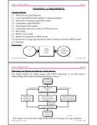
Create successful ePaper yourself
Turn your PDF publications into a flip-book with our unique Google optimized e-Paper software.
Chapter 6 – Section 5 (5/2/04) Page 6.5-16<br />
Frequency Response of the Folded Cascode Op Amp<br />
The frequency response of the folded cascode op amp is determined primarily by the<br />
output pole which is given as<br />
p out =<br />
-1<br />
R out C out<br />
where C out is all the capacitance connected from the output of the op amp to ground.<br />
All other poles must be greater than GB = g m1 /C out . The approximate expressions for<br />
each pole is<br />
1.) Pole at node A: p A ≈ - g m6 /C A<br />
2.) Pole at node B: p B ≈ - g m7 /C B<br />
3.) Pole at drain of M6: p 6 ≈<br />
-1<br />
(R 2 +1/g m10 )C 6<br />
4.) Pole at source of M8: p 8 ≈ -g m8 /C 8<br />
5.) Pole at source of M9: p 9 ≈ -g m9 /C 9<br />
6.) Pole at gate of M10: p 10 ≈ -g m10 /C 10<br />
where the approximate expressions are found by the reciprocal product of the resistance<br />
and parasitic capacitance seen to ground from a given node. One might feel that because<br />
R B is approximately r ds that this pole might be too small. However, at frequencies where<br />
this pole has influence, C out , causes R out to be much smaller making p B also non-dominant.<br />
CMOS <strong>Analog</strong> Circuit <strong>Design</strong> © P.E. Allen - 2004<br />
Chapter 6 – Section 5 (5/2/04) Page 6.5-17<br />
Example 6.5-3 - Folded Cascode, CMOS Op Amp<br />
Assume that all g mN = g mP = 100µS, r dsN = 2MΩ, r dsP = 1MΩ, and C L = 10pF. Find all<br />
of the small-signal performance values for the folded-cascode op amp.<br />
R II = 0.4GΩ, R A = 10kΩ, and R B = 4MΩ<br />
v out<br />
∴ k = 0.4x10 9(0.3x10⁻⁶)<br />
100 = 1.2<br />
⎛2+1.2⎞<br />
v = ⎜ ⎟<br />
in ⎝ 2+2.4 (100)(57.143) = 4,156V/V<br />
⎠<br />
R out = R II ||[g m7 r ds7 (r ds5 ||r ds2 )] = 400MΩ||[(100)(0.667MΩ)] = 57.143MΩ<br />
1<br />
1<br />
|p out | = R out C out<br />
= 57.143MΩ·10pF = 1,750 rads/sec. ⇒ 278Hz ⇒ GB = 1.21MHz<br />
CMOS <strong>Analog</strong> Circuit <strong>Design</strong> © P.E. Allen - 2004