Create successful ePaper yourself
Turn your PDF publications into a flip-book with our unique Google optimized e-Paper software.
Chapter 6 – Section 5 (5/2/04) Page 6.5-4<br />
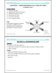
Two-Stage Op Amp with a Cascoded First-Stage<br />
MC3<br />
R<br />
M3<br />
MB3<br />
V DD<br />
M4<br />
MB4<br />
MC4<br />
v o1<br />
MT2<br />
MT1<br />
C c<br />
M6<br />
v out<br />
MB5<br />
MC1 +<br />
MC2<br />
M1 M2<br />
VBias<br />
MB1 MB2<br />
+ -<br />
vin -<br />
v in<br />
2 -<br />
+ 2<br />
+<br />
M5<br />
VBias<br />
-<br />
V SS<br />
CMOS <strong>Analog</strong> Circuit <strong>Design</strong> © P.E. Allen - 2004<br />
M7<br />
Fig. 6.5-2<br />
• MT1 and MT2 are required for level shifting from<br />
the first-stage to the second.<br />
• The PSRR+ is improved by the presence of MT1 p2<br />
• Internal loop pole at the gate of M6 may cause the<br />
Miller compensation to fail.<br />
• The voltage gain of this op amp could easily be 100,000V/V<br />
jω<br />
σ<br />
p 3 p 1<br />
z 1<br />
Fig. 6.5-2<br />
Chapter 6 – Section 5 (5/2/04) Page 6.5-5<br />
Two-Stage Op Amp with a Cascode Second-Stage<br />
V DD<br />
M3<br />
M4<br />
R z<br />
VBP<br />
C c<br />
M6<br />
MC6<br />
v out<br />
- M1 M2<br />
v in<br />
+<br />
+<br />
VBias<br />
-<br />
M5<br />
V SS<br />
CMOS <strong>Analog</strong> Circuit <strong>Design</strong> © P.E. Allen - 2004<br />
VBN<br />
MC7<br />
M7<br />
C L<br />
Fig. 6.5-3<br />
A v = g mI g mII R I R II where g mI = g m1 = g m2 , g mII = g m6 ,<br />
1<br />
2<br />
R I = g ds2 + g ds4<br />
= (λ 2 + λ 4 )I D5<br />
and R II = (g mC6 r dsC6 r ds6 )||(g mC7 r dsC7 r ds7 )<br />
Comments:<br />
• The second-stage gain has greatly increased improving the Miller compensation<br />
• The overall gain is approximately (g m r ds )3 or very large<br />
• Output pole, p 2 , is approximately the same if C c is constant<br />
• The zero RHP is the same if C c is constant