
You also want an ePaper? Increase the reach of your titles
YUMPU automatically turns print PDFs into web optimized ePapers that Google loves.
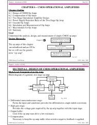
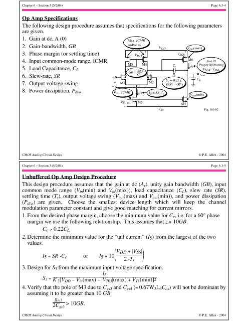
Chapter 6 – Section 3 (5/2/04) Page 6.3-4<br />
Op Amp Specifications<br />
The following design procedure assumes that specifications for the following parameters<br />
are given.<br />
1. Gain at dc, A v (0)<br />
2. Gain-bandwidth, GB<br />
3. Phase margin (or settling time)<br />
4. Input common-mode range, <strong>IC</strong>MR<br />
5. Load Capacitance, C L<br />
6. Slew-rate, SR<br />
-<br />
7. Output voltage swing<br />
+<br />
8. Power dissipation, P diss<br />
Max. <strong>IC</strong>MR<br />
and/or p 3 V DD<br />
+<br />
V V +<br />
V out (max)<br />
SG4 SG6 -<br />
-<br />
M6 g m6 or<br />
M3 M4<br />
C c I 6<br />
Proper Mirroring<br />
V SG4 =V SG6<br />
GB = g m1<br />
C c<br />
v out<br />
C<br />
v L<br />
in<br />
C M1 M2 c ≈ 0.2C L<br />
(PM = 60°)<br />
Min. <strong>IC</strong>MR I 5 I5 = SR·C c V out (min)<br />
+<br />
VBias<br />
-<br />
M5<br />
V SS<br />
M7<br />
Fig. 160-02<br />
CMOS <strong>Analog</strong> Circuit <strong>Design</strong> © P.E. Allen - 2004<br />
Chapter 6 – Section 3 (5/2/04) Page 6.3-5<br />
Unbuffered Op Amp <strong>Design</strong> Procedure<br />
This design procedure assumes that the gain at dc (A v ), unity gain bandwidth (GB), input<br />
common mode range (V in (min) and V in (max)), load capacitance (C L ), slew rate (SR),<br />
settling time (T s ), output voltage swing (V out (max) and V out (min)), and power dissipation<br />
(P diss ) are given. Choose the smallest device length which will keep the channel<br />
modulation parameter constant and give good matching for current mirrors.<br />
1. From the desired phase margin, choose the minimum value for C c , i.e. for a 60° phase<br />
margin we use the following relationship. This assumes that z ≥ 10GB.<br />
C c > 0.22C L<br />
2. Determine the minimum value for the “tail current” (I 5 ) from the largest of the two<br />
values.<br />
I 5 = SR .C c or I 5 ≅ 10⎜ ⎛ V DD + |V SS |<br />
⎝ 2 . ⎠ ⎟⎞<br />
Ts<br />
3. <strong>Design</strong> for S 3 from the maximum input voltage specification.<br />
I 5<br />
S 3 = K' 3 [V DD − V in (max) − |V T03 |(max) + V T1 (min)]2<br />
4. Verify that the pole of M3 due to C gs3 and C gs4 (= 0.67W 3 L 3 C ox ) will not be dominant by<br />
assuming it to be greater than 10 GB<br />
g m3<br />
2C gs3<br />
> 10GB.<br />
CMOS <strong>Analog</strong> Circuit <strong>Design</strong> © P.E. Allen - 2004