book of abstracts - IM2NP
book of abstracts - IM2NP
book of abstracts - IM2NP

Create successful ePaper yourself
Turn your PDF publications into a flip-book with our unique Google optimized e-Paper software.
A B S T R A C T S FRIDAY, JULY 2 N A N O S E A 2 0 1 0<br />
Room Calendal<br />
9H00-9H30<br />
Bottom-up elaboration <strong>of</strong> heterogenous ordered ceramic nanopatterns<br />
substrates for deposition <strong>of</strong> magnetic materials.<br />
D. Grosso*(1), M. Faustini(1), D. Lantiat(1), C. Laberty(1) ((1) Laboratoire Chimie de la<br />
Matiere Condensée de Paris, UMR UPMC-CNRS 7574, Université Pierre et Marie Curie (Paris 6), Collège de<br />
France, 11, place Marcelin Berthelot, 75231 Paris).* presenting author, e-mail: david.grosso@upmc.fr<br />
Ceramic (e.g. semiconducting TiO2, or insulating ZrO2, Al2O3) nanopatterns on various substrates (e.g. Si,<br />
Au, SiO2, Cr) have been prepared through simple fast, cheap, reproducible, and easy to scale up “bottom-up”<br />
approach, involving chemical solution deposition, self-assembly via commercial block copolymers, and<br />
thermal treatment.[1] The patterns is composed <strong>of</strong> hexagonally arranged nanoperforations through which the<br />
surface <strong>of</strong> the substrate remains accessible. The typical thickness <strong>of</strong> the patterns can be controlled between 5<br />
and 20 nm, while a proper selection <strong>of</strong> chemical and processing conditions allows to perfectly adjust the<br />
motif dimension between 10 and 100 nm.[2] They constitute novel highly ordered heterogeneous<br />
Inorganic/inorganic Nano Patterned (INP) substrates, which present a unique combination <strong>of</strong> thermal,<br />
mechanical, and chemical stability with the very interesting characteristics <strong>of</strong> the ordered nano-heterogeneity<br />
associated to the accessibility <strong>of</strong> the substrate surface through the perforations.<br />
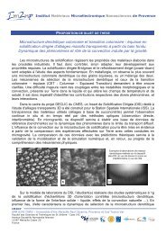
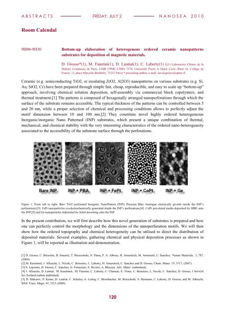
Figure 1. From left to right: Bare TiO2 perforated Inorganic NanoPattern (INP); Prussian Blue Analogue chemically growth inside the INP‟s<br />
perforations;[3] FePt nanoparticles co-electrochemically generated inside the INP‟s perforations;[4] CoPt percolated media deposited by MBE onto<br />
the INP;[5] and Ge nanoparticles elaborated by Solid dewetting onto the INP.<br />
In the present contribution, we will first describe how this novel generation <strong>of</strong> substrates is prepared and how<br />
one can perfectly control the morphology and the dimensions <strong>of</strong> the nanoperforation motifs. We will then<br />
show how the ordered topography and chemical heterogeneity can be utilised to direct the distribution <strong>of</strong><br />
deposited materials. Several examples, gathering chemical and physical deposition processes as shown in<br />
Figure 1, will be reported as illustration and demonstration.<br />
[1] D. Grosso, C. Boissière, B. Smarsly, T. Brezesinski, N. Pinna, P. A. Albouy, H. Amenitsch, M. Antonietti, C. Sanchez, Nature Materials, 3, 787,<br />
(2004).<br />
[2] M. Kuemmel, J. Allouche, L. Nicole, C. Boissière, C. Laberty, H. Amenitsch, C. Sanchez and D. Grosso, Chem. Mater. 19, 3717, (2007).<br />
[3] S. Lepoutre, D. Grosso, C. Sanchez, G. Fornasieri, E. Rivière, A. Bleuzen, Adv. Mater. (submitted).<br />
[4] J. Allouche, D. Lantiat, M. Kuemmel, M. Faustini, C. Laberty, C. Chaneac, E. Tronc, C. Boissiere, L. Nicole, C. Sanchez, D. Grosso, J Sol-Gel<br />
Sci Technol (online published).<br />
[5] D. Makarov, P. Krone, D. Lantiat, C. Schulze, A. Liebig, C. Brombacher, M. Hietschold, S. Hermann, C. Laberty, D. Grosso, and M. Albrecht,<br />
IEEE Trans. Magn. 45, 3515 (2009).<br />
120