book of abstracts - IM2NP
book of abstracts - IM2NP
book of abstracts - IM2NP

Create successful ePaper yourself
Turn your PDF publications into a flip-book with our unique Google optimized e-Paper software.
A B S T R A C T S TUESDAY, JUNE 29 N A N O S E A 2 0 1 0<br />
Results were then discussed on the basis <strong>of</strong> theoretical calculations [8] and density <strong>of</strong> states function<br />
measurement using resonant shell-tunneling Spectroscopy experiments [9]. Only the results related to the 7<br />
nm are reported here.<br />
2 - Results<br />
2-1 Geometry, size and spacing distribution, crystal structure and relative orientation.<br />
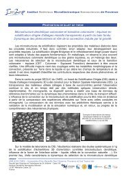
A typical Scanning Transmission Electron Microscope (STEM-FEG-SEM) is displayed in Figure 1. This<br />
images show that the PbSe nanocrystals have a well-controlled size and shape and can locally form ordered<br />
close-packed arrays as indicated from calculated Fast Fourier Transformations (FFT) presented face to face.<br />
In the scheme <strong>of</strong> one NCs layer, hexagonal arrangement is close to be perfect while for NCs bilayers, the<br />
defects introduce by size distribution effect, rapidly break the simple hexagonal arrangement existing locally,<br />
to generate new geometrical stackings i.e. grids, roses. STEM-SEM images are too noisy if observed at the<br />
magnification necessary to make accurate measurements <strong>of</strong> the nanocrystals size. In contrast, TEM images<br />
recorded in High Resolution mode using the Cs objective corrector makes it possible, even at rather low<br />
magnifications. In this mode, one can observe several dozen <strong>of</strong> PbSe NCs which show lattice fringes and<br />
well-defined outlines. It is thus possible to make a rather rapid determination <strong>of</strong> the shape, mean size, size<br />
and spacing distribution. Typical histograms <strong>of</strong> the variation <strong>of</strong> NCs size and spacing between NCs displayed<br />
figure 2, show that NCs size distribution is very narrow. More than 85% <strong>of</strong> the nanocrystals have diameters<br />
ranging between 6.9 and 7.1 nm, with a mean size <strong>of</strong> 7.05 nm. In contrast, NCs spacings distribution is larger<br />
and spreads from 1 to 4 nm with less than 50% equal to 2 nm. HREM images in figure 3, show that most <strong>of</strong><br />
the nanoparticles appear roughly spherical, but some <strong>of</strong> them i.e. thoses with the largest size, show facets.<br />
Therefore, due to projection effects, even spherical nanocrystals can have more or less facetted shapes. Since<br />
some NCs are naturally in [111] or [110] zone axis, the electron diffraction patterns calculated using FFT,<br />
allow to determine that PbSe NCs are face centered cubic (FCC) with a Fm3m space group. Using the<br />
ASTAR s<strong>of</strong>tware, it is possible to make mapping <strong>of</strong> the crystal structure orientation in the transmission<br />
mode, similarly to electron backscattering mapping in the scanning mode. Figure 4 shows the result obtained<br />
for an HRTEM image <strong>of</strong> 39.2 nm 2 scanned with a window <strong>of</strong> 5.7 nm 2 . As indicated by the colour code used<br />
to identify the orientation within the standard triangle, preferential orientations are clearly revealed. It may<br />
be deduced that the z axis is not random but that the particles are free to rotate around. This result is in<br />
agreement with the observations we did locally, which have shown that in close-packed arrays, nanocrystals<br />
tend to form chains along the direction. Such a favoured arrangement had already been predicted and<br />
theoretically explained on the basis <strong>of</strong> dipole moment values reported by Cho et al.[4] but had never clearly<br />
observed.<br />
2-2 Electronic properties <strong>of</strong> single and self-assembled nanocrystals. shows the single scattering distribution<br />
spectra (SSDS) calculated from experimental low-energy loss spectra recorded from a single 7 nm PbSe<br />
nanocrystal and a 2D self-assembled structure composed <strong>of</strong> about fifty PbSe nanocrystals with 7 nm mean<br />
size, deposited on a 30 nm thick Si 3 N 4 film. This spectrum shows numerous features resolved in the very low<br />
energy region (0 - 4 eV), each one corresponding to a more or less sharp intensity jump. As expected, spectra<br />
recorded under similar conditions on the Si 3 N 4 film show the absence <strong>of</strong> structure in the energy range below<br />
4.5 0.1 eV. Only a very weak and uniform background, due to the Bremstralung induces by the NCs<br />
support is observed. Thus, the first sharp intensity jump in the NCs or self-assembled structure spectra<br />
corresponds to E g i.e. the PbSe NCs band gap energy. For both, individual and simple hexagonal selfassembled<br />
NCs an energy equal to 0.67 eV is measured. This value is consistent to those obtained from<br />
absorption measurements performed in parallel on the same slef-assembled samples. These data also well<br />
agree the theoretical values calculated by different authors [5-8-10].<br />
42