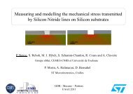
A B S T R A C T S TUESDAY, JUNE 29 N A N O S E A 2 0 1 0 Fig. 2: TEM image <strong>of</strong> a sample obtained after deposition <strong>of</strong> 60 nm <strong>of</strong> Ge on a 25 nm thick Mn5Ge3 layer at 450 °C. A part <strong>of</strong> Mn has diffused into the substrate and the surface Mn5Ge3 layer has a thickness <strong>of</strong> ~17 nm. References [1] O.M.J. van ‟t Erve, G. Kioseoglou, A. T. Hanbicki, C. H. Li, B.T. Jonker, R. Mallory, M. Yasar, A. Petrou, Appl. Phys. Lett 84 (2004) 4334. [2] Y.D. Park, A.T. Hanbicki, S.C. Erwin, C.S. Hellberg, J.M. Sullivan, J.E. Mattson, T.F. Ambrose, A. Wilson, G. Spanos, B.T. Jonker, Science 295 (2002) 651. [3] Y. Ando, K. Hamaya, K. Kasahara, Y. Kishi, K. Ueda, K. Sawano, T. Sadoh, and M. Miyao, Appl. Phys. Lett. 94 (2009) 182105; R. Jaafar, Y. Nehme, D. Berling, J. L. Bubendorff, A. Mehdaoui, C. Pirri, G. Garreau, and C. Uhlaq-Bouillet, Appl. Phys. Lett. 93 (2008) 033114; C. Zeng, S.C. Erwin, L.C. Feldman, A.P. Li, R. Jin, Y. Song, J.R. Thompson, H.H. Weitering, Appl. Phys. Lett. 83, 5002 (2003). [4] S. Olive-mendez, A. Spiesser, L.A. Michez, V. Le Thanh, A. Glachant, J. Derrien, T. Devillers, A. Barski, M. Jamet, Thin Solid Films 517 (2008) 191. [5] A. Spiesser S.F. Olive-Mendez, M.-T. Dau, L.A. Michez, A. Watanabe, V. Le Thanh, A. Glachant, J. Derrien, A. Barski, M. Jamet, Thin Solid Films 518 (2010) S113. 17H40-18H00 Assessing mechanical strain at the nanometer scale induced in silicon channel by periodic gate lines arrays through high resolution X-ray diffraction and modeling S. Escoubas1,2, G. Gaudeau1,2, Y. Ezzaidi1,2, O. Thomas1,2, P. Morin3 (1 Aix- Marseille Université, <strong>IM2NP</strong>; 2 CNRS, <strong>IM2NP</strong> UMR 6242, Faculté des Sciences et Techniques, Campus de Saint- Jérôme, Avenue Escadrille Normandie Niemen, Case 142, 13397 Marseille Cedex, France; 3 ST Microelectronics, 850 rue Jean Monnet, 38920 Crolles, France) stephanie.escoubas@im2np.fr 1 – Introduction Periodic structures are <strong>of</strong>ten encountered in semiconductor devices whether they are prepared by lithography or by self-organization. The lateral dimension <strong>of</strong> the devices is continuously decreasing with increasing performances. Stress engineering is becoming <strong>of</strong> increasing interest to enhance microelectronics device performance in particular by improving electron or hole mobility [1]. For that purpose, one way consists in stressing the transistor Si channel by depositing a strained layer on top <strong>of</strong> the polysilicon gate. Silicon nitride is a good candidate as the layer can be either tensile or compressive depending on the process parameters [2]. Even though the strain field induced in silicon can be predicted with the help <strong>of</strong> finite elements modelling, corroborating the calculated strain field with measurements is crucial. As a consequence, measuring strains or stresses at the nanometer scale is a real challenge. 45
A B S T R A C T S TUESDAY, JUNE 29 N A N O S E A 2 0 1 0 In this study we investigate the periodic strain field in silicon with high resolution X-ray diffraction, which is very sensitive to local strains (
- Page 1 and 2: 3 rd International Conference on NA
- Page 4 and 5: General Information ...............
- Page 6 and 7: NANOSEA 2010 International Conferen
- Page 8: Committees International Scientific
- Page 11 and 12: P R O G R A M MONDAY, JUNE 28 N A N
- Page 13 and 14: A B S T R A C T S MONDAY, JUNE 28 N
- Page 15 and 16: A B S T R A C T S MONDAY, JUNE 28 N
- Page 17 and 18: A B S T R A C T S MONDAY, JUNE 28 N
- Page 19 and 20: A B S T R A C T S MONDAY, JUNE 28 N
- Page 21 and 22: A B S T R A C T S MONDAY, JUNE 28 N
- Page 23 and 24: A B S T R A C T S MONDAY, JUNE 28 N
- Page 25 and 26: A B S T R A C T S MONDAY, JUNE 28 N
- Page 27 and 28: A B S T R A C T S MONDAY, JUNE 28 N
- Page 29 and 30: A B S T R A C T S MONDAY, JUNE 28 N
- Page 31 and 32: P R O G R A M TUESDAY, JUNE 29 N A
- Page 33 and 34: P R O G R A M TUESDAY, JUNE 29 N A
- Page 35 and 36: P R O G R A M TUESDAY, JUNE 29 N A
- Page 37 and 38: A B S T R A C T S TUESDAY, JUNE 29
- Page 39 and 40: A B S T R A C T S TUESDAY, JUNE 29
- Page 41 and 42: A B S T R A C T S TUESDAY, JUNE 29
- Page 43 and 44: A B S T R A C T S TUESDAY, JUNE 29
- Page 45: A B S T R A C T S TUESDAY, JUNE 29
- Page 49 and 50: A B S T R A C T S TUESDAY, JUNE 29
- Page 51 and 52: A B S T R A C T S TUESDAY, JUNE 29
- Page 53 and 54: A B S T R A C T S TUESDAY, JUNE 29
- Page 55 and 56: A B S T R A C T S TUESDAY, JUNE 29
- Page 57 and 58: A B S T R A C T S TUESDAY, JUNE 29
- Page 59 and 60: P R O G R A M WEDNESDAY, JUNE 30 N
- Page 61 and 62: P R O G R A M WEDNESDAY, JUNE 30 N
- Page 63 and 64: A B S T R A C T S WEDNESDAY, JUNE 3
- Page 65 and 66: A B S T R A C T S WEDNESDAY, JUNE 3
- Page 67 and 68: A B S T R A C T S WEDNESDAY, JUNE 3
- Page 69 and 70: A B S T R A C T S WEDNESDAY, JUNE 3
- Page 71 and 72: A B S T R A C T S WEDNESDAY, JUNE 3
- Page 73 and 74: A B S T R A C T S WEDNESDAY, JUNE 3
- Page 75 and 76: A B S T R A C T S WEDNESDAY, JUNE 3
- Page 77 and 78: A B S T R A C T S WEDNESDAY, JUNE 3
- Page 79 and 80: A B S T R A C T S WEDNESDAY, JUNE 3
- Page 81 and 82: P R O G R A M THURSDAY, JULY 1 N A
- Page 83 and 84: P R O G R A M THURSDAY, JULY 1 N A
- Page 85 and 86: P R O G R A M THURSDAY, JULY 1 N A
- Page 87 and 88: P R O G R A M THURSDAY, JULY 1 N A
- Page 89 and 90: P R O G R A M THURSDAY, JULY 1 N A
- Page 91 and 92: A B S T R A C T S THURSDAY, JULY 1
- Page 93 and 94: A B S T R A C T S THURSDAY, JULY 1
- Page 95 and 96: A B S T R A C T S THURSDAY, JULY 1
- Page 97 and 98:
A B S T R A C T S THURSDAY, JULY 1
- Page 99 and 100:
A B S T R A C T S THURSDAY, JULY 1
- Page 101 and 102:
A B S T R A C T S THURSDAY, JULY 1
- Page 103 and 104:
A B S T R A C T S THURSDAY, JULY 1
- Page 105 and 106:
A B S T R A C T S THURSDAY, JULY 1
- Page 107 and 108:
A B S T R A C T S THURSDAY, JULY 1
- Page 109 and 110:
A B S T R A C T S THURSDAY, JULY 1
- Page 111 and 112:
A B S T R A C T S THURSDAY, JULY 1
- Page 113 and 114:
A B S T R A C T S THURSDAY, JULY 1
- Page 115 and 116:
A B S T R A C T S THURSDAY, JULY 1
- Page 117 and 118:
P R O G R A M FRIDAY, JULY 2 N A N
- Page 119 and 120:
P R O G R A M FRIDAY, JULY 2 N A N
- Page 121 and 122:
A B S T R A C T S FRIDAY, JULY 2 N
- Page 123 and 124:
A B S T R A C T S FRIDAY, JULY 2 N
- Page 125 and 126:
A B S T R A C T S FRIDAY, JULY 2 N
- Page 127 and 128:
A B S T R A C T S FRIDAY, JULY 2 N
- Page 129 and 130:
Absorbance (a.u.) Absorbance (a.u.)
- Page 131 and 132:
A B S T R A C T S FRIDAY, JULY 2 N
- Page 133 and 134:
A B S T R A C T S FRIDAY, JULY 2 N
- Page 135 and 136:
A B S T R A C T S FRIDAY, JULY 2 N
- Page 137 and 138:
A B S T R A C T S FRIDAY, JULY 2 N
- Page 139 and 140:
A B S T R A C T S FRIDAY, JULY 2 N
- Page 141 and 142:
140