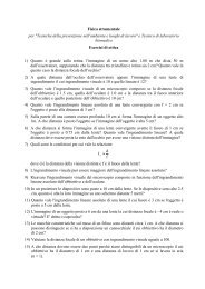
48 CHAPTER 2. EXPERIMENTAL METHODSthe oscillation amplitude; instead, by inspecting the oscillation phase variations it can beachieved a better contrast on material surface <strong>properties</strong>, such as stiffness, viscoelasticity,<strong>and</strong> chemical composition [182–186].The AFM setup employed in this work was composed <strong>of</strong> a Multimode Scanning ProbeMicroscope (fig. 2.10(a), maximum scan size 15μm) driven by a Nanoscope IV controller,both produced by Digital Instruments-Veeco, <strong>and</strong> all the images were acquired in tappingmode; an example is shown in fig. 2.10(b).[001]a. b.Figure 2.10: Panel a: picture <strong>of</strong> a Multimode Scanning Probe Microscope. Panel b: AFMimage <strong>of</strong> a 6 nm Au film on a nanopatterned LiF(110) acquired in tapping mode.
Chapter 3Self-<strong>organized</strong> nanoparticle<strong>arrays</strong>: morphological aspectsIn this chapter we present the procedures for the fabrication <strong>of</strong> lithium fluoride nanostructuredsubstrates <strong>and</strong> for the subsequent realization <strong>of</strong> ordered 2D <strong>arrays</strong> <strong>of</strong> metallicnanoparticles.3.1 Growth <strong>and</strong> characterization <strong>of</strong> lithium fluoridesubstratesWideb<strong>and</strong>gapinsulatorshavebeenextensivelyemployedastemplatesfortheguidedovergrowth<strong>of</strong> metallic structures since a long time [105, 117–121]. Insulating surfaces providea complete electronic decoupling, thus metallic adsorbates can develop a local electronicstructure with specific functionality depending on the growth conditions. Moreover, wideb<strong>and</strong> gap solids are transparent from the near-UV to the near-IR range, so they easilyallow the investigation <strong>of</strong> the optical <strong>properties</strong> <strong>of</strong> the adsorbates, are quite stable in atmosphere,do not suffer oxidation (but in some cases are hygroscopic), <strong>and</strong> are usuallynot magnetic.Ionic crystals, such as NaCl, LiF, MgO, CaF 2 , KBr, are a class <strong>of</strong> insulators composed<strong>of</strong> alternating ions <strong>of</strong> opposite sign. The ions are bound together mainly by electrostaticattractions, so the electrostatic energy strongly affects the stability <strong>of</strong> the surfaces, makingcertain crystal orientations highly favoured. This peculiarity is commonly exploited forthe patterning <strong>of</strong> surfaces at nanoscale [105, 117–121]: when the crystal is cut along anunfavourable direction <strong>and</strong> the atoms are given enough mobility, the less stable surfacescan undergo faceting in favour <strong>of</strong> the more stable orientations, spontaneously leading tothe formation <strong>of</strong> regular structures. For example, faceting into ridges or pyramids, or theformation <strong>of</strong> regular ridge-<strong>and</strong>-valley structures are common phenomena observed uponthermal annealing or homoepitaxy on NaCl(111) [105], NaCl(110) [122, 187], LiF(110)[121], CaF 2 (110) [121] or MgO(110) [106].Inthisthesis, weinvestigated<strong>and</strong>characterizedthehomoepitaxialgrowthonLiF(110).LiF crystals are composed <strong>of</strong> Li + <strong>and</strong> F − ions arranged on a rocksalt cubic structure, witheach ion surrounded by 6 ions <strong>of</strong> the other species (fig. 3.1). The preferential orientations<strong>of</strong> the crystals are the {100} surfaces, consisting <strong>of</strong> alternating ions arranged on a squarelattice (fig. 3.1(c)). {110} surfaces are instead less symmetric <strong>and</strong> less stable, the ions49