Morphology and plasmonic properties of self-organized arrays of ...
Morphology and plasmonic properties of self-organized arrays of ...
Morphology and plasmonic properties of self-organized arrays of ...

You also want an ePaper? Increase the reach of your titles
YUMPU automatically turns print PDFs into web optimized ePapers that Google loves.
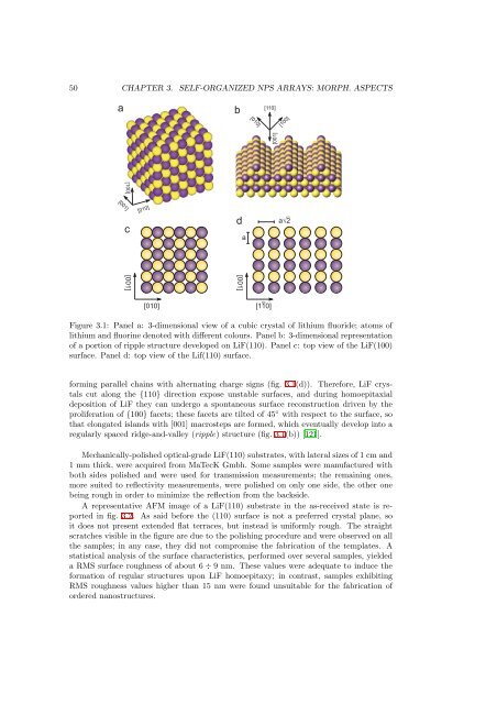
[001][100]50 CHAPTER 3. SELF-ORGANIZED NPS ARRAYS: MORPH. ASPECTSab[010][110][100][001][001]c[010]daa√2[001][010][110]Figure 3.1: Panel a: 3-dimensional view <strong>of</strong> a cubic crystal <strong>of</strong> lithium fluoride; atoms <strong>of</strong>lithium <strong>and</strong> fluorine denoted with different colours. Panel b: 3-dimensional representation<strong>of</strong> a portion <strong>of</strong> ripple structure developed on LiF(110). Panel c: top view <strong>of</strong> the LiF(100)surface. Panel d: top view <strong>of</strong> the Lif(110) surface.forming parallel chains with alternating charge signs (fig. 3.1(d)). Therefore, LiF crystalscut along the {110} direction expose unstable surfaces, <strong>and</strong> during homoepitaxialdeposition <strong>of</strong> LiF they can undergo a spontaneous surface reconstruction driven by theproliferation <strong>of</strong> {100} facets; these facets are tilted <strong>of</strong> 45 ◦ with respect to the surface, sothat elongated isl<strong>and</strong>s with [001] macrosteps are formed, which eventually develop into aregularly spaced ridge-<strong>and</strong>-valley (ripple) structure (fig. 3.1(b)) [121].Mechanically-polished optical-grade LiF(110) substrates, with lateral sizes <strong>of</strong> 1 cm <strong>and</strong>1 mm thick, were acquired from MaTecK Gmbh. Some samples were manufactured withboth sides polished <strong>and</strong> were used for transmission measurements; the remaining ones,more suited to reflectivity measurements, were polished on only one side, the other onebeing rough in order to minimize the reflection from the backside.A representative AFM image <strong>of</strong> a LiF(110) substrate in the as-received state is reportedin fig. 3.2. As said before the (110) surface is not a preferred crystal plane, soit does not present extended flat terraces, but instead is uniformly rough. The straightscratches visible in the figure are due to the polishing procedure <strong>and</strong> were observed on allthe samples; in any case, they did not compromise the fabrication <strong>of</strong> the templates. Astatistical analysis <strong>of</strong> the surface characteristics, performed over several samples, yieldeda RMS surface roughness <strong>of</strong> about 6÷9 nm. These values were adequate to induce theformation <strong>of</strong> regular structures upon LiF homoepitaxy; in contrast, samples exhibitingRMS roughness values higher than 15 nm were found unsuitable for the fabrication <strong>of</strong>ordered nanostructures.