Mechanics and Tribology of MEMS Materials - prod.sandia.gov ...
Mechanics and Tribology of MEMS Materials - prod.sandia.gov ...
Mechanics and Tribology of MEMS Materials - prod.sandia.gov ...
You also want an ePaper? Increase the reach of your titles
YUMPU automatically turns print PDFs into web optimized ePapers that Google loves.
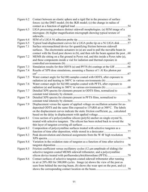
Figure 6.2 Contact between an elastic sphere <strong>and</strong> a rigid flat in the presence <strong>of</strong> surface<br />
forces: (a) the DMT model; (b) the JKR model; (c) the change in radius <strong>of</strong><br />
contact as a function <strong>of</strong> applied load ........................................................................54<br />
Figure 6.3 LIGA processing <strong>prod</strong>uces distinct sidewall morphologies. (a) SEM image <strong>of</strong> a<br />
microgear, (b) higher magnification micrograph showing typical texture <strong>of</strong><br />
sidewalls....................................................................................................................55<br />
Figure 6.4 SEM <strong>of</strong> a LIGA Ni adhesion probe tip .....................................................................56<br />
Figure 6.5 Typical load-displacement curves for a LIGA probe tip on a Ni LIGA disk ...........57<br />
Figure 7.1 Surface micromachined device for quantifying friction between sidewall<br />
surfaces. The electrostatic actuators in (a) are used to pull the movable beam in<br />
contact with the fixed post shown in (b), <strong>and</strong> then rub the beam against the post ...60<br />
Figure 7.2 <strong>MEMS</strong> die sitting on a flat ground in Pyrex rod, <strong>and</strong> this inside a Pyrex tube (a),<br />
<strong>and</strong> these components inside a vial for radiation <strong>and</strong> thermal exposure in<br />
controlled environments (b)......................................................................................62<br />
Figure 7.3 Simulation results for thin ODTS (a) <strong>and</strong> PFTS (b) coatings at the GIF..................66<br />
Figure 7.4 Results <strong>of</strong> XPS dose simulations, assuming a fluence <strong>of</strong> 1 Al Kα photon per<br />
cm 2 ............................................................................................................................67<br />
Figure 7.5 Water contact angle for Si(100) samples coated with ODTS, after exposure to<br />
radiation (a) <strong>and</strong> heating to 300°C in various environments (b) ..............................68<br />
Figure 7.6 Water contact angle for Si(100) samples coated with PFTS, after exposure to<br />
radiation (a) <strong>and</strong> heating to 300°C in various environments (b) ..............................68<br />
Figure 7.7 Detailed XPS spectra for elements present in ODTS films, normalized to<br />
constant total intensity by element............................................................................70<br />
Figure 7.8 Detailed XPS spectra for elements present in PFTS films, normalized to<br />
constant total intensity by element............................................................................71<br />
Figure 7.9 Displacement versus the square <strong>of</strong> applied voltage on oscillation actuator for asdeposited<br />
ODTS <strong>and</strong> the same film exposed to 13%RH air at 300°C. The labels<br />
on the displacement curves indicate the static friction coefficient, µS , calculated<br />
based on the delay in displacement with applied voltage.........................................72<br />
Figure 8.1 Cross section <strong>of</strong> a polycrystalline silicon (polySi) anchor on single crystal Si,<br />
treated with selective tungsten. The silicon has been etched back to reveal the<br />
thin layer <strong>of</strong> tungsten covering all surfaces ..............................................................76<br />
Figure 8.2 Composition <strong>of</strong> polycrystalline surfaces treated with selective tungsten as a<br />
function <strong>of</strong> time after deposition, while stored in a desiccator.................................77<br />
Figure 8.3 Peak deconvolution <strong>and</strong> chemical assignments from the W 4F high resolution<br />
XPS spectra...............................................................................................................78<br />
Figure 8.4 Variation in the oxidation state <strong>of</strong> tungsten as a function <strong>of</strong> time after selective<br />
tungsten deposition ...................................................................................................78<br />
Figure 8.5 Friction coefficient versus oscillatory cycles (12 µm amplitude <strong>of</strong> sliding) for<br />
selective tungsten coated <strong>MEMS</strong> sidewall tribometer, <strong>and</strong> a polycrystalline<br />
silicon device treated with perfluorodecyltrichlorosilane (PFTS)............................79<br />
Figure 8.6 Contact surfaces <strong>of</strong> selective tungsten coated sidewall tribometer after running<br />
in air at 20% RH for 300,000 cycles. Image (a) shows the view <strong>of</strong> the post as<br />
seen from behind the moving beam, (b) shows the wear spot on the post, <strong>and</strong> (c)<br />
shows the corresponding contact location on the beam............................................79<br />
11


