Mechanics and Tribology of MEMS Materials - prod.sandia.gov ...
Mechanics and Tribology of MEMS Materials - prod.sandia.gov ...
Mechanics and Tribology of MEMS Materials - prod.sandia.gov ...

Create successful ePaper yourself
Turn your PDF publications into a flip-book with our unique Google optimized e-Paper software.
Dose/(Equilibrium Dose)<br />
1.25<br />
1.20<br />
1.15<br />
1.10<br />
1.05<br />
1.00<br />
0.1 1 10 100<br />
ODTS Layer Thickness (nm)<br />
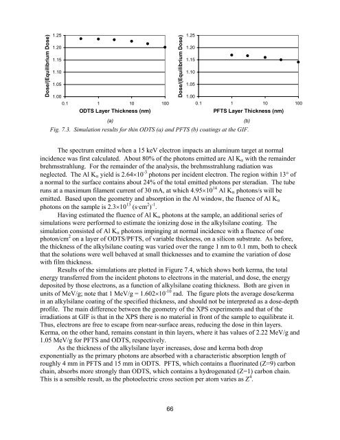
Fig. 7.3. Simulation results for thin ODTS (a) <strong>and</strong> PFTS (b) coatings at the GIF.<br />
The spectrum emitted when a 15 keV electron impacts an aluminum target at normal<br />
incidence was first calculated. About 80% <strong>of</strong> the photons emitted are Al Kα with the remainder<br />
brehmsstrahlung. For the remainder <strong>of</strong> the analysis, the brehmsstrahlung radiation was<br />
neglected. The Al Kα yield is 2.64×10 -3 photons per incident electron. The region within 13° <strong>of</strong><br />
a normal to the surface contains about 24% <strong>of</strong> the total emitted photons per steradian. The tube<br />
runs at a maximum filament current <strong>of</strong> 30 mA, at which 4.95×10 14 Al Kα photons/s will be<br />
emitted. Based upon the geometry <strong>and</strong> absorption in the Al window, the fluence <strong>of</strong> Al Kα<br />
photons on the sample is 2.3×10 13 (s·cm 2 ) -1 .<br />
Having estimated the fluence <strong>of</strong> Al Kα photons at the sample, an additional series <strong>of</strong><br />
simulations were performed to estimate the ionizing dose in the alkylsilane coating. The<br />
simulation consisted <strong>of</strong> Al Kα photons impinging at normal incidence with a fluence <strong>of</strong> one<br />
photon/cm 2 on a layer <strong>of</strong> ODTS/PFTS, <strong>of</strong> variable thickness, on a silicon substrate. As before,<br />
the thickness <strong>of</strong> the alkylsilane coating was varied over the range 1 nm to 0.1 mm, both to check<br />
that the solutions were well behaved at small thicknesses <strong>and</strong> to examine the variation <strong>of</strong> dose<br />
with film thickness.<br />
Results <strong>of</strong> the simulations are plotted in Figure 7.4, which shows both kerma, the total<br />
energy transferred from the incident photons to electrons in the material, <strong>and</strong> dose, the energy<br />
deposited by those electrons, as a function <strong>of</strong> alkylsilane coating thickness. Both are given in<br />
units <strong>of</strong> MeV/g; note that 1 MeV/g = 1.602×10 -10 rad. The figure plots the average dose/kerma<br />
in an alkylsilane coating <strong>of</strong> the specified thickness, <strong>and</strong> should not be interpreted as a dose-depth<br />
pr<strong>of</strong>ile. The main difference between the geometry <strong>of</strong> the XPS experiments <strong>and</strong> that <strong>of</strong> the<br />
irradiations at GIF is that in the XPS there is no material in front <strong>of</strong> the sample to equilibrate it.<br />
Thus, electrons are free to escape from near-surface areas, reducing the dose in thin layers.<br />
Kerma, on the other h<strong>and</strong>, remains constant in thin layers, where it has values <strong>of</strong> 2.22 MeV/g <strong>and</strong><br />
1.05 MeV/g for PFTS <strong>and</strong> ODTS, respectively.<br />
As the thickness <strong>of</strong> the alkylsilane layer increases, dose <strong>and</strong> kerma both drop<br />
exponentially as the primary photons are absorbed with a characteristic absorption length <strong>of</strong><br />
roughly 4 mm in PFTS <strong>and</strong> 15 mm in ODTS. PFTS, which contains a fluorinated (Z=9) carbon<br />
chain, absorbs more strongly than ODTS, which contains a hydrogenated (Z=1) carbon chain.<br />
This is a sensible result, as the photoelectric cross section per atom varies as Z 4 .<br />
66<br />
Dose/(Equilibrium Dose)<br />
1.25<br />
1.20<br />
1.15<br />
1.10<br />
1.05<br />
1.00<br />
0.1 1 10 100<br />
PFTS Layer Thickness (nm)<br />
(a) (b)