Mechanics and Tribology of MEMS Materials - prod.sandia.gov ...
Mechanics and Tribology of MEMS Materials - prod.sandia.gov ...
Mechanics and Tribology of MEMS Materials - prod.sandia.gov ...

Create successful ePaper yourself
Turn your PDF publications into a flip-book with our unique Google optimized e-Paper software.
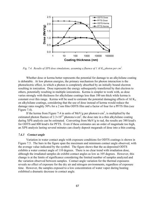
Dose (MeV/g)<br />
Fig. 7.4. Results <strong>of</strong> XPS dose simulations, assuming a fluence <strong>of</strong> 1 Al Kα photon per cm 2 .<br />
Whether dose or kerma better represents the potential for damage to an alkylsilane coating<br />
is debatable. At low photon energies, the primary mechanism for photon interaction is the<br />
photoelectric effect, in which a photon is completely absorbed by an initially bound electron<br />
resulting in ionization. Dose represents the energy subsequently transferred by that electron to<br />
others, potentially resulting in multiple ionizations. Kerma is simpler to work with, as dose<br />
varies strongly with thickness for alkylsilane coatings less than 100 nm thick while kerma is<br />
constant over this range. Kerma will be used to estimate the potential damaging effects <strong>of</strong> Al Kα<br />
on alkylsilane coatings, considering that the use <strong>of</strong> dose instead <strong>of</strong> kerma would reduce the<br />
damage rates roughly 50% for a 2 nm film ODTS film <strong>and</strong> a factor <strong>of</strong> four for a PFTS film (see<br />
Figure 7.4).<br />
If the kerma from Figure 7.4 in units <strong>of</strong> MeV/g per photon/s·cm 2 , is multiplied by the<br />
estimated photon fluence <strong>of</strong> 2.3×10 13 photons/s·cm 2 , the dose rate in a thin alkylsilane coating<br />
during XPS analysis can be estimated. Converting from MeV/g to rad, the results are 380 krad/s<br />
for ODTS <strong>and</strong> 800 krad/s for PFTS. Even if these estimates are an order <strong>of</strong> magnitude too high,<br />
an XPS analysis lasting several minutes can clearly deposit megarads <strong>of</strong> dose into a thin coating.<br />
7.4.3 Contact angle<br />
2.5<br />
2.0<br />
1.5<br />
1.0<br />
0.5<br />
0.0<br />
1 10 100 1000 10000 100000<br />
Coating thickness (nm)<br />
Variation in water contact angle with exposure conditions for ODTS coatings is shown in<br />
Figure 7.5. The bars in the figure span the maximum <strong>and</strong> minimum contact angle observed, with<br />
the average value indicated by the symbol. The figure shows that the as-deposited ODTS<br />
exhibits a water contact angle <strong>of</strong> 110 degrees. There is no clear trend with irradiation dose,<br />
although the irradiated samples do exhibit contact angles as low as 105 degrees. However, this<br />
change is at the limits <strong>of</strong> significance considering the limited number <strong>of</strong> samples analyzed <strong>and</strong><br />
the variation observed between samples. Contact angle variation for the thermal exposures<br />
reveals no effect <strong>of</strong> exposure for the dry air <strong>and</strong> nitrogen environments, regardless <strong>of</strong> exposure<br />
time. However, the samples exposed to a low concentration <strong>of</strong> water vapor during heating<br />
exhibited a dramatic decrease in contact angle.<br />
67<br />
ODTS Dose<br />
PFTS Dose<br />
ODTS Kerma<br />
PFTS Kerma