RK06/RK07 Disk Drive User's Manual - Trailing-Edge
RK06/RK07 Disk Drive User's Manual - Trailing-Edge
RK06/RK07 Disk Drive User's Manual - Trailing-Edge

You also want an ePaper? Increase the reach of your titles
YUMPU automatically turns print PDFs into web optimized ePapers that Google loves.
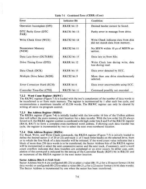
Error<br />
Operation Incomplete (OPI)<br />
DTC Parity Error (DTC<br />
PAR)<br />
Write Check Error (WCE)<br />
Nonexistent Memory<br />
(NEM)<br />
Data Late Error (DLTERR)<br />
<strong>Drive</strong> Timing Error (DTE)<br />
Data Check (DCK)<br />
Multiple <strong>Drive</strong> Select (M DS)<br />
Error Correction Hard (ECH)<br />
Controller Time-Out (CTO)<br />
Table 7-1 Combined Error (CERR) (Cont)<br />
Indicator Bit<br />
RKER bit 13<br />
RKCSI bit 13<br />
RKCS2 bit 14<br />
RKCS2 bit 11<br />
RKCS2 bit 15<br />
RKER bit 12<br />
RKER bit 15<br />
RKCS2 bit 9<br />
RKER bit 6<br />
RKCSI bit II<br />
Condition<br />
Desired header cannot be found.<br />
Parity error in message from drive.<br />
Write Check indicates data from disk<br />
did not match data from memory.<br />
No SSYN within 10 JlS of MSYN assertion.<br />
Data late to /from Silo.<br />
Write Clock loss during write, data<br />
loss during read.<br />
Data error detected by ECC.<br />
More than one drive simultaneously<br />
selected.<br />
Data error un correctable using ECC.<br />
Command possibly not executed.<br />
7.2.2 Word Count Register (RKWC)<br />
The RK WC register (Figure 7-3) is loaded with the two's complement of the number of data words to<br />
be transferred to or from main memory. The register is incremented by 1 after each bus cycle, and<br />
accommodates a maximum transfer of 65,536 words. The RKWC register can only be cleared by<br />
writing all zeros via program control.<br />
7.2.3 Bus Address Register (RKBA)<br />
The RKBA register (Figure 7-4) is initially loaded with the low-order 16 bits of the Unibus address<br />
that will reflect the main memory start location for a data transfer. With the low-order bit (0) always<br />
forced to 0, the RKBA register content is combined with high-order bits 8 and 9 of the RKCS 1 register<br />
(BA 16, BAI7) to form a complete even-numbered word address. Following each data transfer bus<br />
cycle, the register is incremented by two to select the next even-numbered location.<br />
7.2.4 <strong>Disk</strong> Address Register (RKDA)<br />
For Read, Write, and Write Check commands, the RKDA register (Figure 7-5) is initially loaded to<br />
define the desired sector (1 of 20 or 22) and track (l of 3 read/write heads) on the selected drive, from<br />
or to which the first block of a data transfer will be initiated. If the word count value indicates that a<br />
block of more than 256 data words is to be transferred, the Sector Address bits of the RKDA register<br />
will be incremented to select the next consecutive sector and the next track, if necessary, until a word<br />
count overflow indicates that data transfers are completed or an error occurs. In either case, completion<br />
of the command is indicated by the setting of the Controller Ready (RDY) bit in RKCS 1 and<br />
an increment of the RKDA register to the next sector location.<br />
Sector Address Bits 0-4 (SAO-SA4)<br />
Sector Address bits 0-4 are configured (00-23) to select a value (00-19 19) for a 20-sector format (18-bit<br />
data words) or configured (00-25) to select a value (00-2119) for a 22-sector format (l6-bit data words).<br />
The Sector Address is incremented by one when the sector has been transferred.<br />
7-6