Single-Chip Low Power RF Transceiver for Narrowband Systems ...
Single-Chip Low Power RF Transceiver for Narrowband Systems ...
Single-Chip Low Power RF Transceiver for Narrowband Systems ...

You also want an ePaper? Increase the reach of your titles
YUMPU automatically turns print PDFs into web optimized ePapers that Google loves.
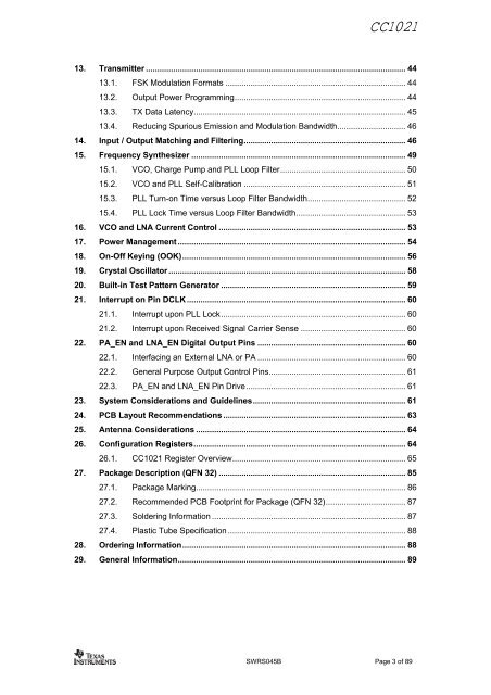
CC1021<br />
13. Transmitter .................................................................................................................. 44<br />
13.1. FSK Modulation Formats ............................................................................... 44<br />
13.2. Output <strong>Power</strong> Programming........................................................................... 44<br />
13.3. TX Data Latency............................................................................................. 45<br />
13.4. Reducing Spurious Emission and Modulation Bandwidth.............................. 46<br />
14. Input / Output Matching and Filtering....................................................................... 46<br />
15. Frequency Synthesizer .............................................................................................. 49<br />
15.1. VCO, Charge Pump and PLL Loop Filter....................................................... 50<br />
15.2. VCO and PLL Self-Calibration ....................................................................... 51<br />
15.3. PLL Turn-on Time versus Loop Filter Bandwidth........................................... 52<br />
15.4. PLL Lock Time versus Loop Filter Bandwidth................................................ 53<br />
16. VCO and LNA Current Control .................................................................................. 53<br />
17. <strong>Power</strong> Management .................................................................................................... 54<br />
18. On-Off Keying (OOK).................................................................................................. 56<br />
19. Crystal Oscillator ........................................................................................................ 58<br />
20. Built-in Test Pattern Generator ................................................................................. 59<br />
21. Interrupt on Pin DCLK ................................................................................................ 60<br />
21.1. Interrupt upon PLL Lock................................................................................. 60<br />
21.2. Interrupt upon Received Signal Carrier Sense .............................................. 60<br />
22. PA_EN and LNA_EN Digital Output Pins ................................................................. 60<br />
22.1. Interfacing an External LNA or PA ................................................................. 60<br />
22.2. General Purpose Output Control Pins............................................................ 61<br />
22.3. PA_EN and LNA_EN Pin Drive...................................................................... 61<br />
23. System Considerations and Guidelines................................................................... 61<br />
24. PCB Layout Recommendations ................................................................................ 63<br />
25. Antenna Considerations ............................................................................................ 64<br />
26. Configuration Registers............................................................................................. 64<br />
26.1. CC1021 Register Overview............................................................................ 65<br />
27. Package Description (QFN 32) .................................................................................. 85<br />
27.1. Package Marking............................................................................................ 86<br />
27.2. Recommended PCB Footprint <strong>for</strong> Package (QFN 32)................................... 87<br />
27.3. Soldering In<strong>for</strong>mation ..................................................................................... 87<br />
27.4. Plastic Tube Specification .............................................................................. 88<br />
28. Ordering In<strong>for</strong>mation.................................................................................................. 88<br />
29. General In<strong>for</strong>mation.................................................................................................... 89<br />
SWRS045B Page 3 of 89