Single-Chip Low Power RF Transceiver for Narrowband Systems ...
Single-Chip Low Power RF Transceiver for Narrowband Systems ...
Single-Chip Low Power RF Transceiver for Narrowband Systems ...

Create successful ePaper yourself
Turn your PDF publications into a flip-book with our unique Google optimized e-Paper software.
LNA_EN and PA_EN are used to control the external T/R switch.<br />
22.2. General Purpose Output Control Pins<br />
CC1021<br />
The two digi tal output pins, PA_EN<br />
and is controlled by LOCK_SELECT[3:0]<br />
in the<br />
LN A_EN, can be used as two<br />
general LOCK<br />
register. The LOCK pin is low when<br />
control signals by setting EXT_PA = 0 and LOCK_SELECT[3:0]<br />
= 0000, and high<br />
EXT_LNA = 0. The output value<br />
is then when<br />
LOCK_SELECT[3:0] = 0001.<br />
set directly by the value written to<br />
EXT_PA_POL and EXT_LNA_POL. These<br />
features can be used to save I/O<br />
pins<br />
on the microcontroller when the other<br />
The LO CK pin can also be used as a functions<br />
associated with these pins are<br />
general- purpose output pin. The<br />
LOCK pin not used.<br />
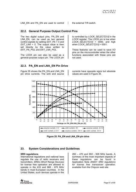
22.3. PA_EN and LNA_EN Pin Drive<br />
Figure 35 shows the PA_EN and<br />
LNA_EN currents<br />
have opposite<br />
signs but absolute<br />
pin drive current s. The sink and source values<br />
are used in Figure 35.<br />
Current [uA]<br />
1400<br />
1200<br />
1000<br />
800<br />
600<br />
400<br />
200<br />
0<br />
0<br />
0.2<br />
0.4<br />
0.6<br />
0.8<br />
1<br />
1.2<br />
1.4<br />
1.6<br />
1.8<br />
2<br />
2.2<br />
2.4<br />
Voltage on PA_EN/LNA_EN pin [V]<br />
source current, 3 V sink current, 3V source current, 2.3 V<br />
sink current, 2.3 V source current, 3.6 V sink current, 3.6 V<br />
2.6<br />
Figure<br />
35. PA_EN and LNA_EN pin drive<br />
23. System Considerations and Guidelines<br />
SRD regulations International regulations and<br />
national<br />
laws<br />
regulate<br />
the use of radio receivers<br />
and<br />
transmitters.<br />
SRDs (Short Range Devices)<br />
<strong>for</strong> license free operation are allowed to<br />
operate in the 433 and 868 - 870 MHz<br />
bands in most European countries. In the<br />
United States, such devices operate in the<br />
2.8<br />
3<br />
3.2<br />
3.4<br />
3.6<br />
260 – 470 and 902 - 928 MHz bands. A<br />
summary<br />
of the most<br />
important aspects of<br />
these<br />
regulations can be found in<br />
Application Note AN001 SRD regulations<br />
<strong>for</strong> license free transceiver operation,<br />
available from the <strong>Chip</strong>con web site.<br />
SWRS045B Page 61 of 89