Single-Chip Low Power RF Transceiver for Narrowband Systems ...
Single-Chip Low Power RF Transceiver for Narrowband Systems ...
Single-Chip Low Power RF Transceiver for Narrowband Systems ...

Create successful ePaper yourself
Turn your PDF publications into a flip-book with our unique Google optimized e-Paper software.
6. Circuit Description<br />
<strong>RF</strong>_IN LNA<br />
<strong>RF</strong>_OUT<br />
PA<br />
LNA 2<br />
<strong>Power</strong><br />
Control<br />
PA_EN LNA_EN<br />
Multiplexer<br />
BIAS<br />
0<br />
:2<br />
90<br />
Multiplexer<br />
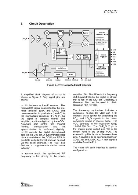
A simplified block diagram of CC1021 is<br />
shown in Figure 2. Only signal pins are<br />
shown.<br />
CC1021 features a low-IF receiver. The<br />
received<br />
<strong>RF</strong> signal is amplified by the low-<br />
noise<br />
amplifier (LNA and LNA2) and<br />
down-converted in quadrature (I and Q) to<br />
the intermediate frequency (IF). At IF, the<br />
I/Q signal is complex filtered and<br />
amplified, and then digitized by the ADCs.<br />
Automatic gain control, fine channel<br />
filtering, demodulation and bit<br />
synchronization is per<strong>for</strong>med digitally.<br />
CC1021 outputs the digital demodulated<br />
data on the DIO pin. A synchronized data<br />
clock is available at the DCLK pin. RSSI is<br />
available in digital <strong>for</strong>mat and can be read<br />
via the serial interface. The RSSI also<br />
features a programmable carrier sense<br />
indicator.<br />
In transmit mode, the synthesized <strong>RF</strong><br />
frequency is fed directly to the power<br />
0<br />
90 :2<br />
XOSC<br />
R_BIAS XOSC_Q1 XOSC_Q2<br />
ADC<br />
ADC<br />
FREQ<br />
SYNTH<br />
VC CHP_OUT<br />
Figure 2. CC1021 simplified<br />
block diagram<br />
DIGITAL<br />
DEMODULATOR<br />
- Digital RSSI<br />
- Gain Control<br />
- Image Suppression<br />
- Channel Filtering<br />
- Demodulation<br />
CONTROL<br />
LOGIC<br />
DIGITAL<br />
MODULATOR<br />
- Modulation<br />
- Data shaping<br />
- <strong>Power</strong> Control<br />
CC1021<br />
DIGITAL<br />
INTE<strong>RF</strong>ACE<br />
TO µC<br />
LOCK<br />
DIO<br />
DCLK<br />
PDO<br />
PDI<br />
PCLK<br />
PSEL<br />
amplifier (PA). The <strong>RF</strong> output is frequency<br />
shift keyed (FSK) by the digital bit stream<br />
that is fed to the DIO pin. Optionally, a<br />
Gaussian filter can be used to obtain<br />
Gaussian FSK (GFSK).<br />
The frequency synthesizer includes a<br />
completely on-chip LC VCO and a 90<br />
degrees phase splitter <strong>for</strong> generating the<br />
LO_I and LO_Q signals to the downconversion<br />
mixers in receive mode. The<br />
VCO operates in the frequency range<br />
1.608-1.880 GHz. The CHP_OUT pin is<br />
the charge pump output and VC is the<br />
control node of the on-chip VCO. The<br />
external loop filter is placed between these<br />
pins. A crystal is to be connected between<br />
XOSC_Q1 and XOSC_Q2. A lock signal is<br />
available from the PLL.<br />
The 4-wire SPI serial interface is used <strong>for</strong><br />
configuration.<br />
SWRS045B Page 17 of 89