Single-Chip Low Power RF Transceiver for Narrowband Systems ...
Single-Chip Low Power RF Transceiver for Narrowband Systems ...
Single-Chip Low Power RF Transceiver for Narrowband Systems ...

Create successful ePaper yourself
Turn your PDF publications into a flip-book with our unique Google optimized e-Paper software.
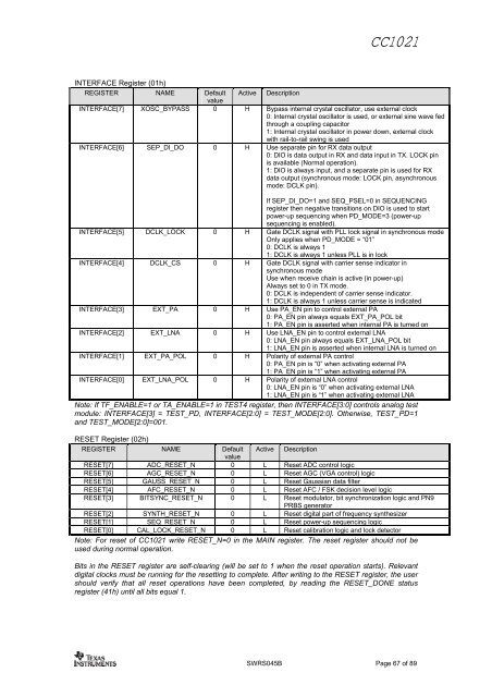
CC1021<br />
INTE<strong>RF</strong>ACE Register (01h)<br />
REGISTER NAME Default<br />
value<br />
Active Description<br />
INTE<strong>RF</strong>ACE[ 7] XOSC_BYPASS 0 H Byp ass internal crystal oscillator, use external clock<br />
0: Internal crystal oscillator<br />
is used, or external sine wave fed<br />
through a coupling capacitor<br />
1: Internal crystal oscillator in power down, external<br />
clock<br />
with rail-to-rail swing is used<br />
INTE<strong>RF</strong>ACE[6] SEP_DI_DO 0 H Use separate pin <strong>for</strong> RX data output<br />
0: D IO is data output in RX and data input in TX.<br />
LOCK pin<br />
is available<br />
(Normal operation).<br />
1: DIO is always input, and a separate pin is used<br />
<strong>for</strong> RX<br />
data<br />
output (synchronous mode: LOCK pin, asynchronous<br />
mode: DCLK pin).<br />
INTE<strong>RF</strong>ACE[ 5] DCLK_LOCK 0 H<br />
If SEP_DI_DO=1<br />
and SEQ_PSEL=0 in SEQUENCING<br />
register<br />
then negative transitions on DIO is used to start<br />
power-up sequencing when PD_MODE=3 (power-up<br />
seq uencing is enabled) .<br />
Gate DCLK signal with PLL lock signal in synchronous mode<br />
Only applies when PD_MODE<br />
= “01”<br />
0: DCLK<br />
is always 1<br />
1: DCLK<br />
is always 1 unless PLL is in lock<br />
INTE<strong>RF</strong>ACE[4] DCLK_CS 0 H Gate DCLK signal with carrier sense indicator in<br />
synchronous<br />
mode<br />
Use when receive chain is active (in power-up)<br />
Always<br />
set to 0 in TX mode.<br />
0: DCLK is independent of carrier sense indicator.<br />
1: D CLK is always 1 unless carrier sense is indicated<br />
INTE<strong>RF</strong>ACE[3] EXT_PA 0 H Use PA_EN pin to control external PA<br />
0: PA_EN<br />
pin always equals EXT_PA_POL bit<br />
1: PA_EN pin is asserted when internal PA is turned on<br />
INTE<strong>RF</strong>ACE[2] EXT_LNA 0 H Use LNA_EN pin to control external LNA<br />
0: LNA_EN pin always equals EXT_LNA_POL bit<br />
1: LNA_EN pin is asserted when internal LNA is turned on<br />
INTE<strong>RF</strong>ACE[1] EXT_PA_POL 0 H Polarity of external PA control<br />
0: PA_EN pin<br />
is “0” when activating external PA<br />
1: PA_EN pin<br />
is “1” when activating external PA<br />
INTE<strong>RF</strong>ACE[0] E XT_LNA_POL 0 H Polarity of external LNA control<br />
0: LNA_EN pin is “0” when activating external<br />
LNA<br />
1: LNA_EN pin is “1” when activating external<br />
LNA<br />
Note: If TF_ENABLE=1<br />
or TA_ENABLE=<br />
1 in TEST4 regi ster, then INTE<strong>RF</strong>ACE[3:0] controls analog test<br />
module: INTE<strong>RF</strong>ACE[3]<br />
= TEST_PD,<br />
INTE<strong>RF</strong>ACE[2:0] = TEST_MODE[2:0]. Otherwise, TEST_PD=1<br />
and TEST_MODE[2:0]=001.<br />
RESET Register (02h)<br />
REGISTER NAME Default<br />
value<br />
Active Description<br />
RESET[7] ADC_RESET_N 0 L Reset ADC control logic<br />
RESET[6] AGC_RESET_N 0 L Reset AGC (VGA control) logic<br />
RESET[5] GAUSS_RESET_N 0 L Reset Gaussian data filter<br />
RESET[4] AFC_RESET_N 0 L Reset AFC / FSK decision level logic<br />
RESET[3] BITSYNC_RESET_N 0 L Reset modulator, bit synchronization<br />
logic and PN9<br />
PRBS generator<br />
RESET[2] SYNTH_RESET_N 0 L Reset digital part of frequency synthesizer<br />
RESET[1] SEQ_RESET_N 0 L Reset power-up sequencing logic<br />
RESET[0] CAL_LOCK_RESET_N 0 L Reset calibration logic and lock detector<br />
Note: For reset of CC1021 write RESET_N=0 in the MAIN<br />
register. The reset register should not be<br />
used during normal operation.<br />
Bits<br />
in the RESET register are self-clearing (will be set to 1 when the reset operation starts). Relevant<br />
digital clocks must be running <strong>for</strong> the resetting to complete. After writing to the RESET register, the user<br />
should verify that all reset operations have been completed, by reading the RESET_DONE status<br />
register (41h) until all bits equal 1.<br />
SWRS045B Page 67 of 89