technical manual for sailor compact hf ssb t2130 - Gopher Proxy
technical manual for sailor compact hf ssb t2130 - Gopher Proxy
technical manual for sailor compact hf ssb t2130 - Gopher Proxy
Create successful ePaper yourself
Turn your PDF publications into a flip-book with our unique Google optimized e-Paper software.
T2130<br />
5 CIRCUIT DESCRIPTION AND SCHEMATIC DIAGRAMS<br />
5.1 POWER AMPLIFIER (MODULE 1) PART NO. 625641<br />
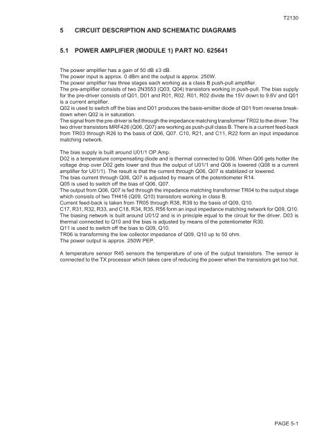
The power amplifier has a gain of 50 dB ±3 dB.<br />
The power input is approx. 0 dBm and the output is approx. 250W.<br />
The power amplifier has three stages each working as a class B push-pull amplifier.<br />
The pre-amplifier consists of two 2N3553 (Q03, Q04) transistors working in push-pull. The bias supply<br />
<strong>for</strong> the pre-driver consists of Q01, D01 and R01, R02. R01, R02 divide the 15V down to 9.6V and Q01<br />
is a current amplifier.<br />
Q02 is used to switch off the bias and D01 produces the basis-emitter diode of Q01 from reverse breakdown<br />
when Q02 is in saturation.<br />
The signal from the pre-driver is fed through the impedance matching trans<strong>for</strong>mer TR02 to the driver. The<br />
two driver transistors MRF426 (Q06, Q07) are working as push-pull class B. There is a current feed-back<br />
from TR03 through R26 to the basis of Q06, Q07. C10, R21, and C11, R22 <strong>for</strong>m an input impedance<br />
matching network.<br />
The bias supply is built around U01/1 OP.Amp.<br />
D02 is a temperature compensating diode and is thermal connected to Q06. When Q06 gets hotter the<br />
voltage drop over D02 gets lower and thus the output of U01/1 and Q08 is lowered (Q08 is a current<br />
amplifier <strong>for</strong> U01/1). The result is that the current through Q06, Q07 is stabilized or lowered.<br />
The bias current through Q06, Q07 is adjusted by means of the potentiometer R14.<br />
Q05 is used to switch off the bias of Q06, Q07.<br />
The output from Q06, Q07 is fed through the impedance matching trans<strong>for</strong>mer TR04 to the output stage<br />
which consists of two TH416 (Q09, Q10) transistors working in class B.<br />
Current feed-back is taken from TR05 through R38, R39 to the basis of Q09, Q10.<br />
C17, R31, R32, R33, and C18, R34, R35, R56 <strong>for</strong>m an input impedance matching network <strong>for</strong> Q09, Q10.<br />
The biasing network is built around U01/2 and is in principle equal to the circuit <strong>for</strong> the driver. D03 is<br />
thermal connected to Q10 and the bias is adjusted by means of the potentiometer R30.<br />
Q11 is used to switch off the bias to Q09, Q10.<br />
TR06 is trans<strong>for</strong>ming the low collector impedance of Q09, Q10 up to 50 ohm.<br />
The power output is approx. 250W PEP.<br />
A temperature sensor R45 sensors the temperature of one of the output transistors. The sensor is<br />
connected to the TX processor which takes care of reducing the power when the transistors get too hot.<br />
PAGE 5-1


