Jahresbericht 2005 - IPHT Jena
Jahresbericht 2005 - IPHT Jena
Jahresbericht 2005 - IPHT Jena

Create successful ePaper yourself
Turn your PDF publications into a flip-book with our unique Google optimized e-Paper software.
MAGNETIK & QUANTENELEKTRONIK / MAGNETICS & QUANTUM ELECTRONICS<br />
1.2 Scientific results<br />
1.2.1 Micro- and nanofabrication<br />
(Uwe Hübner, Ludwig Fritzsch,<br />
Solveig Anders, Jürgen Kunert)<br />
The microfabrication group is responsible for the<br />
maintenance of the existing micro- and nanotechnological<br />
fabrication processes for quantum<br />
electronic devices (SQUID sensors, voltage standard<br />
chips, Qubits) and other applications such<br />
as nanoscale calibration standards, photonic<br />
crystals and micro optical components, and for<br />
the development of technologies appropriate for<br />
new device requirements. In <strong>2005</strong>, 210 chromium<br />
masks and 240 electron beam direct writing<br />
exposure jobs were made using the ZBA 23H.<br />
120 masks were prepared by using the optical<br />
pattern generator MANN 3600. About 80 high<br />
resolution exposures were made using the<br />
e-beam-tool LION. For the further improvement<br />
of the electron beam lithography the software<br />
tool SCELETON was installed as a proximity<br />
function calculator.<br />
In <strong>2005</strong> a new DFG-project, “Electrooptically Tunable<br />
Photonic Crystals”, was started. The European<br />
project PLATON (PLAnar Technology for<br />
Optical Networks) and the R&D project “KALI II”<br />
were successfully finished. In the “KALI II” project<br />
a new type of nanoscale CD-standard for AFM<br />
and a “Nanoscale Linewidth/Pitch Standard”<br />
were realized. These standards consist of different<br />
grating structures etched in nanocrystalline<br />
silicon on a quartz substrate. They contain<br />
patterns on nanometer scale for the calibration<br />
and resolution-check of high-resolution optical<br />
microscopy techniques, such as deep ultraviolet<br />
microscopy and laser scanning microscopy.<br />
One important task of the year <strong>2005</strong> was to<br />
develop a process to reduce the standard 3.5 µm 2<br />
Nb/Al process to junction dimensions of 1 µm 2 .At<br />
the start of <strong>2005</strong> a chemical-mechanical polishing<br />
(CMP) machine was installed and the process<br />
of SiO 2-planarization on 4” wafers developed. In<br />
parallel, optical lithography using a g-line stepper<br />
(AÜR, Zeiss <strong>Jena</strong>) and the RIE process for sub-<br />
µm Nb structures were optimized. A first wafer<br />
run with test structures of SQUIDs with Josephson<br />
junctions of different dimensions down to 0.8<br />
µm showed in principal the functionality of the<br />
planarization process. However, there was a<br />
large parameter spread and a small yield, caused<br />
by an insufficient reliability and overlap accuracy<br />
of the stepper and the strong dependence of the<br />
polishing rate on topology and structure dimensions.<br />
Therefore, for the ongoing test runs new<br />
technological concepts were developed including<br />
direct e-beam exposure and the CALDERA<br />
process for the CMP step in order to overcome<br />
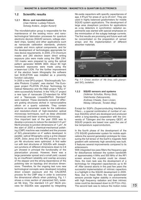
the dimensional effects when polishing. Fig. 1.1<br />
shows a cross section of planarized SiO 2 isolated<br />
Nb lines. The standard 3.5 µm 2 Nb/Al process<br />
for SQUIDs was upgraded by integrating<br />
Nb-oxide capacitors with specific capacitances of<br />
app. 4 fF/µm 2 for areas of up to 25 mm 2 . They are<br />
used in highly balanced gradiometers for mobile<br />
SQUID system applications. The development of<br />
large area Josephson junctions for applications<br />
as x-ray detectors in synchrotron radiation experiments<br />
was started with special emphasize on<br />
the minimization of the subgap leakage currents.<br />
The first results are promising and future work will<br />
be concentrated on the preparation of sensor<br />
arrays and the implementation of different<br />
absorber materials.<br />
Fig. 1.1: Cross section of Nb lines with planarized<br />
SiO 2 isolation.<br />
1.2.2 SQUID sensors and systems<br />
(Volkmar Schultze, Ronny Stolz,<br />
Viatcheslav Zakosarenko,<br />
Andreas Chwala, Sven Linzen,<br />
Nilolay Ukhanski, Torsten May)<br />
Except for SQIFs (Superconducting Interference<br />
Filters – a special combination of number of various<br />
SQUIDs) which are developed and produced<br />
within a long-standing cooperation with the University<br />
of Tübingen and the company QEST, all<br />
SQUID projects are based now upon the use of<br />
low temperature superconductors.<br />
In the fourth phase of the development of the<br />
LTS SQUID gradiometer system for mobile applications<br />
the second generation prototype for measuring<br />
the full tensor of the Earth’s magnetic field<br />
gradient with extremely high sensitivity was built.<br />
It features several improvements compared to its<br />
antecessors.<br />
With integrated low pass filters the frequency gap<br />
for disturbances between the system bandwidth<br />
of approximately 4 MHz and 500 MHz of the RFI<br />
screen around the cryostat could be closed.<br />
Here, the main task was the development of a<br />
technology for integrated capacitances up to 80<br />
nF. After several aborts in the past few years the<br />
successful implementation of intrinsic capacitors<br />
is a highlight in the SQUID development in <strong>2005</strong>.<br />
Now, due to these filters the new gradiometer<br />
sensors provide higher stability in environments<br />
with high frequency radiation and their intrinsic<br />
noise could be decreased down to 20 fT/(m·√Hz).<br />
The second task was to reduce the motion noise<br />
15