Jahresbericht 2005 - IPHT Jena
Jahresbericht 2005 - IPHT Jena
Jahresbericht 2005 - IPHT Jena

You also want an ePaper? Increase the reach of your titles
YUMPU automatically turns print PDFs into web optimized ePapers that Google loves.
92<br />
The varying shades (spectrum from white to<br />
greenish-blue in a colour picture) indicate the different<br />
level of filling and positioning accuracy. In<br />
order to improve the homogeneity a further optimisation<br />
of this technique is required.<br />
Thin film solar cells<br />
For the first time layered laser crystallised (LLC)<br />
thin film solar cells were prepared on borofloat<br />
glass substrates covered with a tantalum pentoxide<br />
layer.<br />
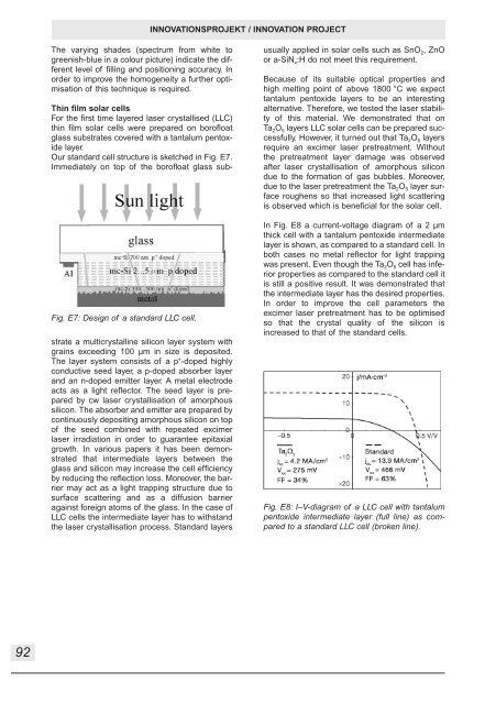
Our standard cell structure is sketched in Fig. E7.<br />
Immediately on top of the borofloat glass sub-<br />
Fig. E7: Design of a standard LLC cell.<br />
strate a multicrystalline silicon layer system with<br />
grains exceeding 100 µm in size is deposited.<br />
The layer system consists of a p + -doped highly<br />
conductive seed layer, a p-doped absorber layer<br />
and an n-doped emitter layer. A metal electrode<br />
acts as a light reflector. The seed layer is prepared<br />
by cw laser crystallisation of amorphous<br />
silicon. The absorber and emitter are prepared by<br />
continuously depositing amorphous silicon on top<br />
of the seed combined with repeated excimer<br />
laser irradiation in order to guarantee epitaxial<br />
growth. In various papers it has been demonstrated<br />
that intermediate layers between the<br />
glass and silicon may increase the cell efficiency<br />
by reducing the reflection loss. Moreover, the barrier<br />
may act as a light trapping structure due to<br />
surface scattering and as a diffusion barrier<br />
against foreign atoms of the glass. In the case of<br />
LLC cells the intermediate layer has to withstand<br />
the laser crystallisation process. Standard layers<br />
INNOVATIONSPROJEKT / INNOVATION PROJECT<br />
usually applied in solar cells such as SnO 2, ZnO<br />
or a-SiN x:H do not meet this requirement.<br />
Because of its suitable optical properties and<br />
high melting point of above 1800 °C we expect<br />
tantalum pentoxide layers to be an interesting<br />
alternative. Therefore, we tested the laser stability<br />
of this material. We demonstrated that on<br />
Ta 2O 5 layers LLC solar cells can be prepared successfully.<br />
However, it turned out that Ta 2O 5 layers<br />
require an excimer laser pretreatment. Without<br />
the pretreatment layer damage was observed<br />
after laser crystallisation of amorphous silicon<br />
due to the formation of gas bubbles. Moreover,<br />
due to the laser pretreatment the Ta 2O 5 layer surface<br />
roughens so that increased light scattering<br />
is observed which is beneficial for the solar cell.<br />
In Fig. E8 a current-voltage diagram of a 2 µm<br />
thick cell with a tantalum pentoxide intermediate<br />
layer is shown, as compared to a standard cell. In<br />
both cases no metal reflector for light trapping<br />
was present. Even though the Ta 2O 5 cell has inferior<br />
properties as compared to the standard cell it<br />
is still a positive result. It was demonstrated that<br />
the intermediate layer has the desired properties.<br />
In order to improve the cell parameters the<br />
excimer laser pretreatment has to be optimised<br />
so that the crystal quality of the silicon is<br />
increased to that of the standard cells.<br />
Fig. E8: I–V-diagram of a LLC cell with tantalum<br />
pentoxide intermediate layer (full line) as compared<br />
to a standard LLC cell (broken line).