Jahresbericht 2005 - IPHT Jena
Jahresbericht 2005 - IPHT Jena
Jahresbericht 2005 - IPHT Jena

You also want an ePaper? Increase the reach of your titles
YUMPU automatically turns print PDFs into web optimized ePapers that Google loves.
Dank besonderem Engagement aller Mitarbeiter<br />
konnte der Bereich Lasertechnik <strong>2005</strong> trotz der<br />
verschärften Situation bei den öffentlichen Fördermitteln<br />
und des allgemein geringen Wirtschaftswachstums<br />
sein Niveau bei den Drittmittelprojekten,<br />
Veröffentlichungen und Patenten wenigstens<br />
in etwa halten. Das Drittmittelaufkommen von rund<br />
1,0 Mio “ liegt merklich unter dem Niveau des Vorjahres<br />
(1,2 Mio “). Insgesamt haben jedoch die<br />
mit dem Umzug erreichten kurzen Wege zu den<br />
anderen <strong>IPHT</strong>-Forschungsbereichen einen deutlichen<br />
Zuwachs bei der bereichsübergreifenden<br />
Zusammenarbeit bewirkt.<br />
4.2 Selected Results<br />
4.2.1 Laser chemistry<br />
Laser chemistry at <strong>IPHT</strong> is essentially concerned<br />
with the deposition of thin films and thin film systems,<br />
their physicochemical modification (particularly<br />
laser crystallisation) and some special<br />
items like spectroscopic diagnostics of thin film<br />
processing, nanowire preparation, and fs laser<br />
micromachining.<br />
Laser crystallisation<br />
(Gudrun Andrä, Joachim Bergmann,<br />
Arne Bochmann, Fritz Falk, Annett Gawlik,<br />
Ekkehardt Ose)<br />
For several years, <strong>IPHT</strong> has been aiming at the<br />
preparation of thin film solar cells consisting of<br />
large grained crystalline silicon on glass. The<br />
development of this new cell type is based on the<br />
deposition of amorphous silicon either by plasma<br />
CVD from SiH 4 (13.6 MHz) or by electron beam<br />
evaporation of bulk silicon and its in situ laser<br />
crystallisation. In a first step large crystal grains<br />
are obtained from 300–500 nm thick amorphous<br />
silicon layers by cw laser crystallisation (seed<br />
layer formation). Subsequently the seed layer<br />
undergoes epitaxial thickening by pulsed Layered<br />
Laser Crystallisation (LLC), an <strong>IPHT</strong> patented<br />
method. So far laboratory cells with an open circuit<br />
voltage of 510 mV and a conversion efficiency<br />
of 4.8% based on an absorber thickness of<br />
5 µm were obtained. Recent work addressed the<br />
acceleration (industrial application) and optimisation<br />
of the seed layer formation by applying a<br />
700 W diode laser focused to a line and scanned<br />
across the substrates to achieve crystallite sizes<br />
of 0.1 to several mm (cf. coloured page). Additional<br />
progress for the solar cell performance is<br />
expected from improving light trapping, improving<br />
contact and shunt resistances as well as minimising<br />
charge carrier recombination. The related<br />
work benefits from the discussions and cooperation<br />
with the Hahn-Meitner-Institute (HMI) at<br />
LASERTECHNIK / LASER TECHNOLOGY<br />
generally poor rate of economic growth. The project<br />
funds in <strong>2005</strong> of about 1.0 Mio are close to<br />
the amount of 2004 (1.2 Mio “). Overall the move<br />
to the Beutenberg campus yielded, however, a<br />
considerable strengthening of trans-divisional<br />
cooperation due to the short distances to the<br />
other <strong>IPHT</strong> research divisions.<br />
Berlin, Solar-Zentrum Erfurt at CiS, Ersol company<br />
at Erfurt, and INPUT Solar, a Thuringian association<br />
of photovoltaic industrial companies and<br />
R&D institutes.<br />
Thin film deposition and nanowire growth<br />
(Gudrun Andrä, Fritz Falk, Herbert Stafast,<br />
Thomas Stelzner)<br />
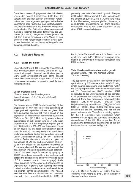
The deposition of Si/C/N thin films for tribological<br />
applications by RF plasma enhanced CVD using<br />
single source precursors was performed within<br />
the DFG program SPP 1119 in close cooperation<br />
with TU Darmstadt and RWTH Aachen. <strong>IPHT</strong><br />
contributed to the understanding of the complex<br />
CVD processes by comparing Si/C/N thin films<br />
obtained from two precursors, hexamethyldisilazane<br />
(CH 3) 3Si-NH-Si(CH 3) 3 (HMDS) and<br />
bis(trimethylsilyl)carbodiimide (CH 3) 3Si-N=C=N-<br />
Si(CH 3) 3 (BTSC). Hard Si/C/N thin films were<br />
obtained on the RF powered, but not on the<br />
grounded electrode. Therefore a heating system<br />
for the RF electrode was developed which<br />
allowed to investigate the substrate temperature<br />
dependence of the thin film properties. As an<br />
example the temperature dependence of the film<br />
hardness is sketched out in Fig. 4.1.<br />
Fig. 4.1: Martens hardness of Si/C/N thin films<br />
obtained from HMDS or BTSC as a function of<br />
the subtrate temperature.<br />
83