CHAPTER 3 METHODOLOGY 3.1 Overview The Water Monitoring ...
CHAPTER 3 METHODOLOGY 3.1 Overview The Water Monitoring ...
CHAPTER 3 METHODOLOGY 3.1 Overview The Water Monitoring ...

You also want an ePaper? Increase the reach of your titles
YUMPU automatically turns print PDFs into web optimized ePapers that Google loves.
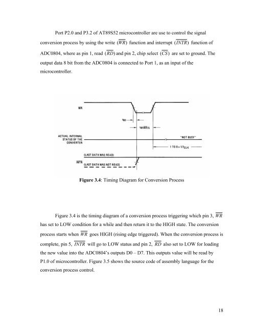
Port P2.0 and P3.2 of AT89S52 microcontroller are use to control the signalconversion process by using the write (WR)function and interrupt (INTR)function ofADC0804, where as pin 1, read (RD)and pin 2, chip select (CS)are set to ground. <strong>The</strong>output data 8 bit from the ADC0804 is connected to Port 1, as an input of themicrocontroller.Figure 3.4: Timing Diagram for Conversion ProcessFigure 3.4 is the timing diagram of a conversion process triggering which pin 3, WRhas set to LOW condition for a while and then return it to the HIGH state. <strong>The</strong> conversionprocess starts when WR goes HIGH (rising edge triggered). When the conversion process iscomplete, pin 5, INTR will go to LOW status and pin 2, RD also set to LOW for loadingthe new value into the ADC0804’s outputs D0 – D7. This outputs value will be read byP1.0 of microcontroller. Figure 3.5 shows the source code of assembly language for theconversion process control.18