CHAPTER 3 METHODOLOGY 3.1 Overview The Water Monitoring ...
CHAPTER 3 METHODOLOGY 3.1 Overview The Water Monitoring ...
CHAPTER 3 METHODOLOGY 3.1 Overview The Water Monitoring ...

Create successful ePaper yourself
Turn your PDF publications into a flip-book with our unique Google optimized e-Paper software.
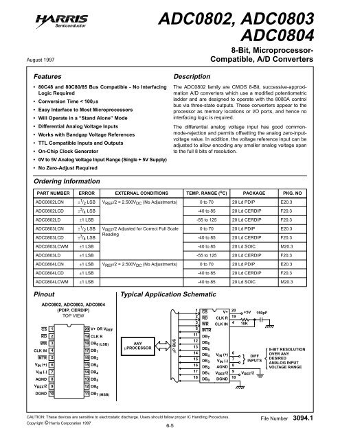
August 1997SemiconductorADC0802, ADC0803ADC08048-Bit, Microprocessor-Compatible, A/D ConvertersFeatures• 80C48 and 80C80/85 Bus Compatible - No InterfacingLogic Required• Conversion Time < 100µs• Easy Interface to Most Microprocessors• Will Operate in a “Stand Alone” Mode• Differential Analog Voltage Inputs• Works with Bandgap Voltage References• TTL Compatible Inputs and Outputs• On-Chip Clock Generator• 0V to 5V Analog Voltage Input Range (Single + 5V Supply)• No Zero-Adjust RequiredDescription<strong>The</strong> ADC0802 family are CMOS 8-Bit, successive-approximationA/D converters which use a modified potentiometricladder and are designed to operate with the 8080A controlbus via three-state outputs. <strong>The</strong>se converters appear to theprocessor as memory locations or I/O ports, and hence nointerfacing logic is required.<strong>The</strong> differential analog voltage input has good commonmode-rejectionand permits offsetting the analog zero-inputvoltagevalue. In addition, the voltage reference input can beadjusted to allow encoding any smaller analog voltage spanto the full 8 bits of resolution.Ordering InformationPART NUMBER ERROR EXTERNAL CONDITIONS TEMP. RANGE ( o C) PACKAGE PKG. NOADC0802LCN ± 1 / 2 LSB V REF /2 = 2.500V DC (No Adjustments) 0 to 70 20 Ld PDIP E20.3ADC0802LCD ± 3 / 4 LSB -40 to 85 20 Ld CERDIP F20.3ADC0802LD ±1 LSB -55 to 125 20 Ld CERDIP F20.3ADC0803LCN ± 1 / 2 LSB V REF /2 Adjusted for Correct Full Scale 0 to 70 20 Ld PDIP E20.3ADC0803LCD ± 3 / 4 LSBReading-40 to 85 20 Ld CERDIP F20.3ADC0803LCWM ±1 LSB -40 to 85 20 Ld SOIC M20.3ADC0803LD ±1 LSB -55 to 125 20 Ld CERDIP F20.3ADC0804LCN ±1 LSB V REF /2 = 2.500V DC (No Adjustments) 0 to 70 20 Ld PDIP E20.3ADC0804LCD ±1 LSB -40 to 85 20 Ld CERDIP F20.3ADC0804LCWM ±1 LSB -40 to 85 20 Ld SOIC M20.3PinoutTypical Application SchematicDB 7 (MSB)ADC0802, ADC0803, ADC0804(PDIP, CERDIP)TOP VIEW12DGND 10113CS 120 V+ OR V REF5RD 219 CLK R1112WR 318 DB 0 (LSB)ANYµPROCESSOR13CLK IN 417 DB 114INTR 516 DB 215V IN (+) 615 DB 316V IN (-) 714 DB 417AGND 813 DB 518V REF /2 912 DB 6µP BUSCSRDWRINTRDB 7DB 6DB 5DB 4DB 3DB 2DB 1DB 0V+CLK RCLK INV IN (+)V IN (-)AGNDV REF /2DGND20194678910+5V10K150pFDIFFINPUTSV REF /28-BIT RESOLUTIONOVER ANYDESIREDANALOG INPUTVOLTAGE RANGECAUTION: <strong>The</strong>se devices are sensitive to electrostatic discharge. Users should follow proper IC Handling Procedures.Copyright © Harris Corporation 19976-5File Number 3094.1