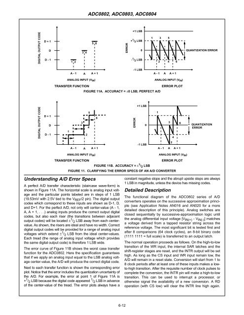
ADC0802, ADC0803, ADC0804DIGITAL OUTPUT CODED + 1DD - 1123 45 6ERROR+1 LSB+ 1 / 2 LSB0- 1 / 2 LSB1 3 52 46* QUANTIZATION ERRORA - 1AA + 1-1 LSBA - 1AA + 1ANALOG INPUT (V IN )ANALOG INPUT (V IN )TRANSFER FUNCTIONERROR PLOTFIGURE 11A. ACCURACY = ±0 LSB; PERFECT A/DDIGITAL OUTPUT CODED + 1DD - 1135426ERROR+1 LSB01346*QUANTIZATIONERRORA - 1AA + 1-1 LSBA - 12A A + 1ANALOG INPUT (V IN )ANALOG INPUT (V IN )TRANSFER FUNCTIONERROR PLOTFIGURE 11B. ACCURACY = ± 1 / 2 LSBFIGURE 11. CLARIFYING THE ERROR SPECS OF AN A/D CONVERTERUnderstanding A/D Error SpecsA perfect A/D transfer characteristic (staircase wave-form) isshown in Figure 11A. <strong>The</strong> horizontal scale is analog input voltageand the particular points labeled are in steps of 1 LSB(19.53mV with 2.5V tied to the V REF /2 pin). <strong>The</strong> digital outputcodes which correspond to these inputs are shown as D-1, D,and D+1. For the perfect A/D, not only will center-value (A - 1,A, A + 1, . . .) analog inputs produce the correct output digitalcodes, but also each riser (the transitions between adjacentoutput codes) will be located ± 1 / 2 LSB away from each centervalue.As shown, the risers are ideal and have no width. Correctdigital output codes will be provided for a range of analog inputvoltages which extend ± 1 / 2 LSB from the ideal center-values.Each tread (the range of analog input voltage which providesthe same digital output code) is therefore 1 LSB wide.<strong>The</strong> error curve of Figure 11B shows the worst case transferfunction for the ADC0802. Here the specification guaranteesthat if we apply an analog input equal to the LSB analog voltagecenter-value, the A/D will produce the correct digital code.Next to each transfer function is shown the corresponding errorplot. Notice that the error includes the quantization uncertainty ofthe A/D. For example, the error at point 1 of Figure 11A is+ 1 / 2 LSB because the digital code appeared 1 / 2 LSB in advanceof the center-value of the tread. <strong>The</strong> error plots always have aconstant negative slope and the abrupt upside steps are always1 LSB in magnitude, unless the device has missing codes.Detailed Description<strong>The</strong> functional diagram of the ADC0802 series of A/Dconverters operates on the successive approximation principle(see Application Notes AN016 and AN020 for a moredetailed description of this principle). Analog switches areclosed sequentially by successive-approximation logic untilthe analog differential input voltage [V lN(+) - V lN(-) ] matchesa voltage derived from a tapped resistor string across thereference voltage. <strong>The</strong> most significant bit is tested first andafter 8 comparisons (64 clock cycles), an 8-bit binary code(1111 1111 = full scale) is transferred to an output latch.<strong>The</strong> normal operation proceeds as follows. On the high-to-lowtransition of the WR input, the internal SAR latches and theshift-register stages are reset, and the INTR output will be sethigh. As long as the CS input and WR input remain low, theA/D will remain in a reset state. Conversion will start from 1 to8 clock periods after at least one of these inputs makes a lowto-hightransition. After the requisite number of clock pulses tocomplete the conversion, the INTR pin will make a high-to-lowtransition. This can be used to interrupt a processor, orotherwise signal the availability of a new conversion. A RDoperation (with CS low) will clear the INTR line high again.6-12
ADC0802, ADC0803, ADC0804<strong>The</strong> device may be operated in the free-running mode by connectingINTR to the WR input with CS = 0. To ensure start-upunder all possible conditions, an external WR pulse is requiredduring the first power-up cycle. A conversion-in-process canbe interrupted by issuing a second start command.Digital Operation<strong>The</strong> converter is started by having CS and WR simultaneouslylow. This sets the start flip-flop (F/F) and the resulting “1” levelresets the 8-bit shift register, resets the Interrupt (INTR) F/Fand inputs a “1” to the D flip-flop, DFF1, which is at the inputend of the 8-bit shift register. Internal clock signals then transferthis “1” to the Q output of DFF1. <strong>The</strong> AND gate, G1, combinesthis “1” output with a clock signal to provide a resetsignal to the start F/F. If the set signal is no longer present(either WR or CS is a “1”), the start F/F is reset and the 8-bitshift register then can have the “1” clocked in, which starts theconversion process. If the set signal were to still be present,this reset pulse would have no effect (both outputs of the startF/F would be at a “1” level) and the 8-bit shift register wouldcontinue to be held in the reset mode. This allows for asynchronousor wide CS and WR signals.After the “1” is clocked through the 8-bit shift register (whichcompletes the SAR operation) it appears as the input toDFF2. As soon as this “1” is output from the shift register, theAND gate, G2, causes the new digital word to transfer to theThree-State output latches. When DFF2 is subsequentlyclocked, the Q output makes a high-to-low transition whichcauses the INTR F/F to set. An inverting buffer then suppliesthe INTR output signal.When data is to be read, the combination of both CS and RDbeing low will cause the INTR F/F to be reset and the threestateoutput latches will be enabled to provide the 8-bit digitaloutputs.Digital Control Inputs<strong>The</strong> digital control inputs (CS, RD, and WR) meet standardTTL logic voltage levels. <strong>The</strong>se signals are essentially equivalentto the standard A/D Start and Output Enable control signals,and are active low to allow an easy interface tomicroprocessor control busses. For non-microprocessorbased applications, the CS input (pin 1) can be grounded andthe standard A/D Start function obtained by an active lowpulse at the WR input (pin 3). <strong>The</strong> Output Enable function isachieved by an active low pulse at the RD input (pin 2).Analog Operation<strong>The</strong> analog comparisons are performed by a capacitivecharge summing circuit. Three capacitors (with precise ratioedvalues) share a common node with the input to an autozeroedcomparator. <strong>The</strong> input capacitor is switched betweenV lN(+) and V lN(-) , while two ratioed reference capacitors areswitched between taps on the reference voltage divider string.<strong>The</strong> net charge corresponds to the weighted differencebetween the input and the current total value set by the successiveapproximation register. A correction is made to offsetthe comparison by 1 / 2 LSB (see Figure 11A).Analog Differential Voltage Inputs and Common-ModeRejectionThis A/D gains considerable applications flexibility from the analogdifferential voltage input. <strong>The</strong> V lN(-) input (pin 7) can be usedto automatically subtract a fixed voltage value from the inputreading (tare correction). This is also useful in 4mA - 20mA currentloop conversion. In addition, common-mode noise can bereduced by use of the differential input.<strong>The</strong> time interval between sampling V IN(+) and V lN(-) is 4 1 / 2clock periods. <strong>The</strong> maximum error voltage due to this slighttime difference between the input voltage samples is given by:4.5∆V E( MAX)= ( V PEAK)( 2πf CM) ------------f CLKwhere:∆V E is the error voltage due to sampling delay,V PEAK is the peak value of the common-mode voltage,f CM is the common-mode frequency.For example, with a 60Hz common-mode frequency, f CM ,and a 640kHz A/D clock, f CLK , keeping this error to 1 / 4 LSB(~5mV) would allow a common-mode voltage, V PEAK , givenby:∆V E( MAX)( fCLK )V PEAK= ------------------------------------------------- ,( 2πf CM )( 4.5)or( 5 × 10 – 3 )( 640 × 10 3 )V PEAK = --------------------------------------------------------- ≅ .( 6.28) ( 60) ( 4.5)1.9V<strong>The</strong> allowed range of analog input voltage usually placesmore severe restrictions on input common-mode voltagelevels than this.An analog input voltage with a reduced span and a relativelylarge zero offset can be easily handled by making use of thedifferential input (see Reference Voltage Span Adjust).Analog Input Current<strong>The</strong> internal switching action causes displacement currents toflow at the analog inputs. <strong>The</strong> voltage on the on-chip capacitanceto ground is switched through the analog differentialinput voltage, resulting in proportional currents entering theV IN(+) input and leaving the V IN(-) input. <strong>The</strong>se current transientsoccur at the leading edge of the internal clocks. <strong>The</strong>yrapidly decay and do not inherently cause errors as the onchipcomparator is strobed at the end of the clock perIod.Input Bypass CapacitorsBypass capacitors at the inputs will average these chargesand cause a DC current to flow through the output resistancesof the analog signal sources. This charge pumping action isworse for continuous conversions with the V IN(+) input voltageat full scale. For a 640kHz clock frequency with the V IN(+)input at 5V, this DC current is at a maximum of approximately5µA. <strong>The</strong>refore, bypass capacitors should not be used atthe analog inputs or the V REF /2 pin for high resistancesources (>1kΩ). If input bypass capacitors are necessary fornoise filtering and high source resistance is desirable to minimizecapacitor size, the effects of the voltage drop across thisinput resistance, due to the average value of the input current,can be compensated by a full scale adjustment while thegiven source resistor and input bypass capacitor are both inplace. This is possible because the average value of the inputcurrent is a precise linear function of the differential inputvoltage at a constant conversion rate.6-13
- Page 1 and 2:
CHAPTER 3METHODOLOGY3.1 OverviewThe
- Page 3 and 4:
3.2.2 Analog To Digital Conversion
- Page 5 and 6:
Figure 3.5: Source Code for Convers
- Page 7 and 8:
3.2.4 Water Monitoring System Circu
- Page 9 and 10:
3.3 Programming.Programming is the
- Page 11 and 12:
ISP flash programmer in Figure 3.11
- Page 13 and 14:
The Visual Basic program will start
- Page 15 and 16:
Distance(cm)ReadingVoltage Trial1 (
- Page 17 and 18:
4.2 Signal ConversionA sensor has s
- Page 19 and 20:
4.3 User InterfaceBased on Table 4.
- Page 21 and 22:
Hardware DesignBasically, the const
- Page 23 and 24:
CHAPTER 5CONCLUSION5.1 SummaryWater
- Page 25 and 26:
This project can be expanded by usi
- Page 27 and 28: APPENDICES41
- Page 29 and 30: cjne a,volt,xsamejmp startxsame:mov
- Page 31 and 32: xsame19:jnc more19mov dptr,#XVALIDc
- Page 33 and 34: etrx:jnb ri,$clr rimov a,sbufretdel
- Page 35 and 36: ElseShape8.FillColor = vbWhiteEnd I
- Page 37 and 38: Private Sub Timer3_Timer()Label3.Ca
- Page 39 and 40: APPENDIX EData Sheet AT89S5253
- Page 41 and 42: Features• Compatible with MCS-51
- Page 43 and 44: AT89S52Block DiagramP0.0 - P0.7P2.0
- Page 45 and 46: AT89S52weakly pulled high. Setting
- Page 47 and 48: AT89S52Table 3a. AUXR: Auxiliary Re
- Page 49 and 50: AT89S52Watchdog Timer(One-time Enab
- Page 51 and 52: AT89S52Figure 6. Timer 2 Auto Reloa
- Page 53 and 54: AT89S52Baud Rate GeneratorTimer 2 i
- Page 55 and 56: AT89S52Oscillator CharacteristicsXT
- Page 57 and 58: AT89S52frequency should be less tha
- Page 59 and 60: Figure 15. Flash Programming and Ve
- Page 61 and 62: AT89S52Table 9. Serial Programming
- Page 63 and 64: AT89S52Absolute Maximum Ratings*Ope
- Page 65 and 66: AT89S52External Program Memory Read
- Page 67 and 68: AT89S52Serial Port Timing: Shift Re
- Page 69 and 70: Packaging Information44A, 44-lead,
- Page 71 and 72: August 1997SemiconductorADC0802, AD
- Page 73 and 74: ADC0802, ADC0803, ADC0804Absolute M
- Page 75 and 76: ADC0802, ADC0803, ADC0804Electrical
- Page 77: ADC0802, ADC0803, ADC0804Typical Pe
- Page 81 and 82: ADC0802, ADC0803, ADC0804V IN ±5VR
- Page 83 and 84: ADC0802, ADC0803, ADC0804Figures 19
- Page 85 and 86: ADC0802, ADC0803, ADC0804IRQ (4)†