ADC0802, ADC0803, ADC0804Electrical Specifications(Notes 1, 7) (Continued)PARAMETER TEST CONDITIONS MIN TYP MAX UNITSCONVERTER SPECIFICATIONS V+ = 5V, -55 o C to 125 o C and f CLK = 640kHz, Unless Otherwise SpecifiedTotal Unadjusted ErrorADC0802 V REF /2 = 2.500V - - ±1 LSBADC0803V REF /2 Adjusted for Correct FullScale Reading- - ±1 LSBV REF /2 Input Resistance Input Resistance at Pin 9 1.0 1.3 - kΩAnalog Input Voltage Range (Note 2) GND-0.05 - (V+) + 0.05 VDC Common-Mode Rejection Over Analog Input Voltage Range - ± 1 / 8 ± 1 / 4 LSBPower Supply Sensitivity V+ = 5V ±10% Over Allowed InputVoltage Range- ± 1 / 8 ± 1 / 4 LSBAC TIMING SPECIFICATIONS V+ = 5V, and T A = 25 o C, Unless Otherwise SpecifiedClock Frequency, f CLK V+ = 6V (Note 3) 100 640 1280 kHzV+ = 5V 100 640 800 kHzClock Periods per Conversion(Note 4), t CONV62 - 73 Clocks/ConvConversion Rate In Free-RunningMode, CRINTR tied to WR with CS = 0V,f CLK = 640kHz- - 8888 Conv/sWidth of WR Input (Start Pulse CS = 0V (Note 5) 100 - - nsWidth), t W(WR)IAccess Time (Delay from FallingEdge of RD to Output Data Valid),t ACCThree-State Control (Delay fromRising Edge of RD to Hl-Z State),t 1H , t 0HC L = 100pF (Use Bus Driver IC for - 135 200 nsLarger C L)C L = 10pF, R L = 10K(See Three-State Test Circuits)- 125 250 nsDelay from Falling Edge of WR to- 300 450 nsReset of INTR, t WI , t RIInput Capacitance of Logic- 5 - pFControl Inputs, C INThree-State Output Capacitance- 5 - pF(Data Buffers), C OUTDC DIGITAL LEVELS AND DC SPECIFICATIONS V+ = 5V, and T MIN to T MAX , Unless Otherwise SpecifiedCONTROL INPUTS (Note 6)Logic “1“ Input Voltage (Except V+ = 5.25V 2.0 - V+ VPin 4 CLK IN), V INHLogic “0“ Input Voltage (Except V+ = 4.75V - - 0.8 VPin 4 CLK IN), V INLCLK IN (Pin 4) Positive Going2.7 <strong>3.1</strong> 3.5 VThreshold Voltage, V+ CLKCLK IN (Pin 4) Negative Going1.5 1.8 2.1 VThreshold Voltage, V- CLKCLK IN (Pin 4) Hysteresis, V H 0.6 1.3 2.0 VLogic “1” Input CurrentV lN = 5V - 0.005 1 µΑ(All Inputs), I INHILogic “0” Input CurrentV lN = 0V -1 -0.005 - µA(All Inputs), I INLOSupply Current (Includes LadderCurrent), I+f CLK = 640kHz,T A = 25 o Cand CS = Hl- 1.3 2.5 mADATA OUTPUTS AND INTRLogic “0” Output Voltage, V OL l O = 1.6mA, V+ = 4.75V - - 0.4 V6-8
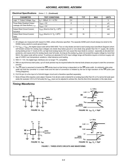
ADC0802, ADC0803, ADC0804Electrical Specifications(Notes 1, 7) (Continued)PARAMETER TEST CONDITIONS MIN TYP MAX UNITSLogic “1” Output Voltage, V OH l O = -360µA, V+ = 4.75V 2.4 - - VThree-State Disabled Output V OUT = 0V -3 - - µALeakage (All Data Buffers), I LO V OUT = 5V - - 3 µAOutput Short Circuit Current,I SOURCEV OUT Short to Gnd T A = 25 o C 4.5 6 - mAOutput Short Circuit Current, V OUT Short to V+ T A = 25 o C 9.0 16 - mAI SINKNOTES:1. All voltages are measured with respect to GND, unless otherwise specified. <strong>The</strong> separate AGND point should always be wired to theDGND, being careful to avoid ground loops.2. For V IN(-) ≥ V IN(+) the digital output code will be 0000 0000. Two on-chip diodes are tied to each analog input (see Block Diagram) whichwill forward conduct for analog input voltages one diode drop below ground or one diode drop greater than the V+ supply. Be careful,during testing at low V+ levels (4.5V), as high level analog inputs (5V) can cause this input diode to conduct - especially at elevated temperatures,and cause errors for analog inputs near full scale. As long as the analog V IN does not exceed the supply voltage by more than50mV, the output code will be correct. To achieve an absolute 0V to 5V input voltage range will therefore require a minimum supply voltageof 4.950V over temperature variations, initial tolerance and loading.3. With V+ = 6V, the digital logic interfaces are no longer TTL compatible.4. With an asynchronous start pulse, up to 8 clock periods may be required before the internal clock phases are proper to start the conversionprocess.5. <strong>The</strong> CS input is assumed to bracket the WR strobe input so that timing is dependent on the WR pulse width. An arbitrarily wide pulsewidth will hold the converter in a reset mode and the start of conversion is initiated by the low to high transition of the WR pulse (seeTiming Diagrams).6. CLK IN (pin 4) is the input of a Schmitt trigger circuit and is therefore specified separately.7. None of these A/Ds requires a zero-adjust. However, if an all zero code is desired for an analog input other than 0V, or if a narrow full scale spanexists (for example: 0.5V to 4V full scale) the V IN(-) input can be adjusted to achieve this. See the Zero Error description in this data sheet.Timing Waveformst r = 20nsV+2.4Vt r90%RDCSC L10KDATAOUTPUTRD0.8VDATAOUTPUTSGND50%10%V OH 90%t 1HFIGURE 1A. t 1HFIGURE 1B. t 1H , C L = 10pFRDCSV+V+10KC LFIGURE 1C. t 0HDATAOUTPUTt r = 20nst r2.4V90%50%RD0.8V10%V+DATAOUTPUTSVOI10%FIGURE 1D. t 0H , C L = 10pFt 0HFIGURE 1. THREE-STATE CIRCUITS AND WAVEFORMS6-9
- Page 1 and 2:
CHAPTER 3METHODOLOGY3.1 OverviewThe
- Page 3 and 4:
3.2.2 Analog To Digital Conversion
- Page 5 and 6:
Figure 3.5: Source Code for Convers
- Page 7 and 8:
3.2.4 Water Monitoring System Circu
- Page 9 and 10:
3.3 Programming.Programming is the
- Page 11 and 12:
ISP flash programmer in Figure 3.11
- Page 13 and 14:
The Visual Basic program will start
- Page 15 and 16:
Distance(cm)ReadingVoltage Trial1 (
- Page 17 and 18:
4.2 Signal ConversionA sensor has s
- Page 19 and 20:
4.3 User InterfaceBased on Table 4.
- Page 21 and 22:
Hardware DesignBasically, the const
- Page 23 and 24: CHAPTER 5CONCLUSION5.1 SummaryWater
- Page 25 and 26: This project can be expanded by usi
- Page 27 and 28: APPENDICES41
- Page 29 and 30: cjne a,volt,xsamejmp startxsame:mov
- Page 31 and 32: xsame19:jnc more19mov dptr,#XVALIDc
- Page 33 and 34: etrx:jnb ri,$clr rimov a,sbufretdel
- Page 35 and 36: ElseShape8.FillColor = vbWhiteEnd I
- Page 37 and 38: Private Sub Timer3_Timer()Label3.Ca
- Page 39 and 40: APPENDIX EData Sheet AT89S5253
- Page 41 and 42: Features• Compatible with MCS-51
- Page 43 and 44: AT89S52Block DiagramP0.0 - P0.7P2.0
- Page 45 and 46: AT89S52weakly pulled high. Setting
- Page 47 and 48: AT89S52Table 3a. AUXR: Auxiliary Re
- Page 49 and 50: AT89S52Watchdog Timer(One-time Enab
- Page 51 and 52: AT89S52Figure 6. Timer 2 Auto Reloa
- Page 53 and 54: AT89S52Baud Rate GeneratorTimer 2 i
- Page 55 and 56: AT89S52Oscillator CharacteristicsXT
- Page 57 and 58: AT89S52frequency should be less tha
- Page 59 and 60: Figure 15. Flash Programming and Ve
- Page 61 and 62: AT89S52Table 9. Serial Programming
- Page 63 and 64: AT89S52Absolute Maximum Ratings*Ope
- Page 65 and 66: AT89S52External Program Memory Read
- Page 67 and 68: AT89S52Serial Port Timing: Shift Re
- Page 69 and 70: Packaging Information44A, 44-lead,
- Page 71 and 72: August 1997SemiconductorADC0802, AD
- Page 73: ADC0802, ADC0803, ADC0804Absolute M
- Page 77 and 78: ADC0802, ADC0803, ADC0804Typical Pe
- Page 79 and 80: ADC0802, ADC0803, ADC0804The device
- Page 81 and 82: ADC0802, ADC0803, ADC0804V IN ±5VR
- Page 83 and 84: ADC0802, ADC0803, ADC0804Figures 19
- Page 85 and 86: ADC0802, ADC0803, ADC0804IRQ (4)†