CHAPTER 3 METHODOLOGY 3.1 Overview The Water Monitoring ...
CHAPTER 3 METHODOLOGY 3.1 Overview The Water Monitoring ...
CHAPTER 3 METHODOLOGY 3.1 Overview The Water Monitoring ...

Create successful ePaper yourself
Turn your PDF publications into a flip-book with our unique Google optimized e-Paper software.
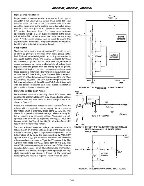
ADC0802, ADC0803, ADC0804Input Source ResistanceLarge values of source resistance where an input bypasscapacitor is not used will not cause errors since the inputcurrents settle out prior to the comparison time. If a lowpassfilter is required in the system, use a low-value seriesresistor (≤1kΩ) for a passive RC section or add an op ampRC active low-pass filter. For low-source-resistanceapplications (≤1kΩ), a 0.1µF bypass capacitor at the inputswill minimize EMI due to the series lead inductance of a longwire. A 100Ω series resistor can be used to isolate thiscapacitor (both the R and C are placed outside the feedbackloop) from the output of an op amp, if used.Stray Pickup<strong>The</strong> leads to the analog inputs (pins 6 and 7) should be keptas short as possible to minimize stray signal pickup (EMI).Both EMI and undesired digital-clock coupling to these inputscan cause system errors. <strong>The</strong> source resistance for theseinputs should, in general, be kept below 5kΩ. Larger values ofsource resistance can cause undesired signal pickup. Inputbypass capacitors, placed from the analog inputs to ground,will eliminate this pickup but can create analog scale errors asthese capacitors will average the transient input switching currentsof the A/D (see Analog Input Current). This scale errordepends on both a large source resistance and the use of aninput bypass capacitor. This error can be compensated by afull scale adjustment of the A/D (see Full Scale Adjustment)with the source resistance and input bypass capacitor inplace, and the desired conversion rate.Reference Voltage Span AdjustFor maximum application flexibility, these A/Ds have beendesigned to accommodate a 5V, 2.5V or an adjusted voltagereference. This has been achieved in the design of the IC asshown in Figure 12.Notice that the reference voltage for the IC is either 1 / 2 of thevoltage which is applied to the V+ supply pin, or is equal tothe voltage which is externally forced at the V REF /2 pin. Thisallows for a pseudo-ratiometric voltage reference using, forthe V+ supply, a 5V reference voltage. Alternatively, a voltageless than 2.5V can be applied to the V REF /2 input. <strong>The</strong>internal gain to the V REF /2 input is 2 to allow this factor of 2reduction in the reference voltage.Such an adjusted reference voltage can accommodate areduced span or dynamic voltage range of the analog inputvoltage. If the analog input voltage were to range from 0.5V to3.5V, instead of 0V to 5V, the span would be 3V. With 0.5Vapplied to the V lN(-) pin to absorb the offset, the referencevoltage can be made equal to 1 / 2 of the 3V span or 1.5V. <strong>The</strong>A/D now will encode the V lN(+) signal from 0.5V to 3.5V withthe 0.5V input corresponding to zero and the 3.5V input correspondingto full scale. <strong>The</strong> full 8 bits of resolution are thereforeapplied over this reduced analog input voltage range. <strong>The</strong> requisiteconnections are shown in Figure 13. For expandedscale inputs, the circuits of Figures 14 and 15 can be used.V REF /2V REF(5V)9RRAGNDDECODEV+(V REF )ANALOGCIRCUITSDIGITALCIRCUITS8 DGND 10FIGURE 12. THE V REFERENCE DESIGN ON THE ICFSADJ.-+5V3000.1µFZERO SHIFT VOLTAGEFIGURE 13. OFFSETTING THE ZERO OF THE ADC0802 ANDPERFORMING AN INPUT RANGE (SPAN)ADJUSTMENTV IN ± 10VICL7611“SPAN”/22RR2R67V IN(-)20TO V REF /2TO V IN(-)5VV IN(+) V+ 20 +(V REF )ADC0802-10µFADC0804FIGURE 14. HANDLING ±10V ANALOG INPUT RANGE6-14