CHAPTER 3 METHODOLOGY 3.1 Overview The Water Monitoring ...
CHAPTER 3 METHODOLOGY 3.1 Overview The Water Monitoring ...
CHAPTER 3 METHODOLOGY 3.1 Overview The Water Monitoring ...
You also want an ePaper? Increase the reach of your titles
YUMPU automatically turns print PDFs into web optimized ePapers that Google loves.
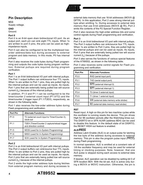
Pin DescriptionVCCSupply voltage.GNDGround.Port 0Port 0 is an 8-bit open drain bidirectional I/O port. As anoutput port, each pin can sink eight TTL inputs. When 1sare written to port 0 pins, the pins can be used as highimpedanceinputs.Port 0 can also be configured to be the multiplexed loworderaddress/data bus during accesses to externalprogram and data memory. In this mode, P0 has internalpullups.Port 0 also receives the code bytes during Flash programmingand outputs the code bytes during program verification.External pullups are required during programverification.Port 1Port 1 is an 8-bit bidirectional I/O port with internal pullups.<strong>The</strong> Port 1 output buffers can sink/source four TTL inputs.When 1s are written to Port 1 pins, they are pulled high bythe internal pullups and can be used as inputs. As inputs,Port 1 pins that are externally being pulled low will sourcecurrent (I IL ) because of the internal pullups.In addition, P1.0 and P1.1 can be configured to be thetimer/counter 2 external count input (P1.0/T2) and thetimer/counter 2 trigger input (P1.1/T2EX), respectively, asshown in the following table.Port 1 also receives the low-order address bytes duringFlash programming and verification.Port PinAlternate FunctionsP1.0 T2 (external count input to Timer/Counter 2),clock-outP1.1 T2EX (Timer/Counter 2 capture/reload triggerand direction control)P1.5 MOSI (used for In-System Programming)P1.6 MISO (used for In-System Programming)P1.7 SCK (used for In-System Programming)Port 2Port 2 is an 8-bit bidirectional I/O port with internal pullups.<strong>The</strong> Port 2 output buffers can sink/source four TTL inputs.When 1s are written to Port 2 pins, they are pulled high bythe internal pullups and can be used as inputs. As inputs,Port 2 pins that are externally being pulled low will sourcecurrent (I IL ) because of the internal pullups.Port 2 emits the high-order address byte during fetchesfrom external program memory and during accesses toexternal data memory that use 16-bit addresses (MOVX @DPTR). In this application, Port 2 uses strong internal pullupswhen emitting 1s. During accesses to external datamemory that use 8-bit addresses (MOVX @ RI), Port 2emits the contents of the P2 Special Function Register.Port 2 also receives the high-order address bits and somecontrol signals during Flash programming and verification.Port 3Port 3 is an 8-bit bidirectional I/O port with internal pullups.<strong>The</strong> Port 3 output buffers can sink/source four TTL inputs.When 1s are written to Port 3 pins, they are pulled high bythe internal pullups and can be used as inputs. As inputs,Port 3 pins that are externally being pulled low will sourcecurrent (I IL ) because of the pullups.Port 3 also serves the functions of various special featuresof the AT89S52, as shown in the following table.Port 3 also receives some control signals for Flash programmingand verification.Port PinAlternate FunctionsP3.0 RXD (serial input port)P<strong>3.1</strong> TXD (serial output port)P3.2 INT0 (external interrupt 0)P3.3 INT1 (external interrupt 1)P3.4 T0 (timer 0 external input)P3.5 T1 (timer 1 external input)P3.6 WR (external data memory write strobe)P3.7 RD (external data memory read strobe)RSTReset input. A high on this pin for two machine cycles whilethe oscillator is running resets the device. This pin drivesHigh for 96 oscillator periods after the Watchdog times out.<strong>The</strong> DISRTO bit in SFR AUXR (address 8EH) can be usedto disable this feature. In the default state of bit DISRTO,the RESET HIGH out feature is enabled.ALE/PROGAddress Latch Enable (ALE) is an output pulse for latchingthe low byte of the address during accesses to externalmemory. This pin is also the program pulse input (PROG)during Flash programming.In normal operation, ALE is emitted at a constant rate of1/6 the oscillator frequency and may be used for externaltiming or clocking purposes. Note, however, that oneALE pulse is skipped during each access to external datamemory.If desired, ALE operation can be disabled by setting bit 0 ofSFR location 8EH. With the bit set, ALE is active only duringa MOVX or MOVC instruction. Otherwise, the pin is4AT89S52


