CHAPTER 3 METHODOLOGY 3.1 Overview The Water Monitoring ...
CHAPTER 3 METHODOLOGY 3.1 Overview The Water Monitoring ...
CHAPTER 3 METHODOLOGY 3.1 Overview The Water Monitoring ...

Create successful ePaper yourself
Turn your PDF publications into a flip-book with our unique Google optimized e-Paper software.
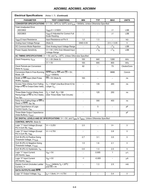
ADC0802, ADC0803, ADC0804Electrical Specifications(Notes 1, 7) (Continued)PARAMETER TEST CONDITIONS MIN TYP MAX UNITSCONVERTER SPECIFICATIONS V+ = 5V, -55 o C to 125 o C and f CLK = 640kHz, Unless Otherwise SpecifiedTotal Unadjusted ErrorADC0802 V REF /2 = 2.500V - - ±1 LSBADC0803V REF /2 Adjusted for Correct FullScale Reading- - ±1 LSBV REF /2 Input Resistance Input Resistance at Pin 9 1.0 1.3 - kΩAnalog Input Voltage Range (Note 2) GND-0.05 - (V+) + 0.05 VDC Common-Mode Rejection Over Analog Input Voltage Range - ± 1 / 8 ± 1 / 4 LSBPower Supply Sensitivity V+ = 5V ±10% Over Allowed InputVoltage Range- ± 1 / 8 ± 1 / 4 LSBAC TIMING SPECIFICATIONS V+ = 5V, and T A = 25 o C, Unless Otherwise SpecifiedClock Frequency, f CLK V+ = 6V (Note 3) 100 640 1280 kHzV+ = 5V 100 640 800 kHzClock Periods per Conversion(Note 4), t CONV62 - 73 Clocks/ConvConversion Rate In Free-RunningMode, CRINTR tied to WR with CS = 0V,f CLK = 640kHz- - 8888 Conv/sWidth of WR Input (Start Pulse CS = 0V (Note 5) 100 - - nsWidth), t W(WR)IAccess Time (Delay from FallingEdge of RD to Output Data Valid),t ACCThree-State Control (Delay fromRising Edge of RD to Hl-Z State),t 1H , t 0HC L = 100pF (Use Bus Driver IC for - 135 200 nsLarger C L)C L = 10pF, R L = 10K(See Three-State Test Circuits)- 125 250 nsDelay from Falling Edge of WR to- 300 450 nsReset of INTR, t WI , t RIInput Capacitance of Logic- 5 - pFControl Inputs, C INThree-State Output Capacitance- 5 - pF(Data Buffers), C OUTDC DIGITAL LEVELS AND DC SPECIFICATIONS V+ = 5V, and T MIN to T MAX , Unless Otherwise SpecifiedCONTROL INPUTS (Note 6)Logic “1“ Input Voltage (Except V+ = 5.25V 2.0 - V+ VPin 4 CLK IN), V INHLogic “0“ Input Voltage (Except V+ = 4.75V - - 0.8 VPin 4 CLK IN), V INLCLK IN (Pin 4) Positive Going2.7 <strong>3.1</strong> 3.5 VThreshold Voltage, V+ CLKCLK IN (Pin 4) Negative Going1.5 1.8 2.1 VThreshold Voltage, V- CLKCLK IN (Pin 4) Hysteresis, V H 0.6 1.3 2.0 VLogic “1” Input CurrentV lN = 5V - 0.005 1 µΑ(All Inputs), I INHILogic “0” Input CurrentV lN = 0V -1 -0.005 - µA(All Inputs), I INLOSupply Current (Includes LadderCurrent), I+f CLK = 640kHz,T A = 25 o Cand CS = Hl- 1.3 2.5 mADATA OUTPUTS AND INTRLogic “0” Output Voltage, V OL l O = 1.6mA, V+ = 4.75V - - 0.4 V6-8