ADC0802, ADC0803, ADC0804150pFSTARTN.O.ANALOGINPUTSADC0802 - ADC0804110K 5V (V REF )CS2 RD CLK R 193 WR DB 0 184 CLK IN DB 1 175 INTR DB 2 166 V IN (+) DB 3 157 V IN (-) DB 4 148 AGND DB 5 139 V REF /2 DB 6 1210 DGND DB 7 11Driving the Data BusThis CMOS A/D, like MOS microprocessors and memories,will require a bus driver when the total capacitance of thedata bus gets large. Other circuItry, which is tied to the databus, will add to the total capacitive loading, even in threestate(high-impedance mode). Back plane busing alsogreatly adds to the stray capacitance of the data bus.<strong>The</strong>re are some alternatives available to the designer to handlethis problem. Basically, the capacitive loading of the databus slows down the response time, even though DC specificationsare still met. For systems operating with a relativelyslow CPU clock frequency, more time is available in which toestablish proper logic levels on the bus and therefore highercapacitive loads can be driven (see Typical PerformanceCurves).At higher CPU clock frequencies time can be extended forI/O reads (and/or writes) by inserting wait states (8080) orusing clock-extending circuits (6800).Finally, if time is short and capacitive loading is high,external bus drivers must be used. <strong>The</strong>se can be three-statebuffers (low power Schottky is recommended, such as the74LS240 series) or special higher-drive-current productswhich are designed as bus drivers. High-current bipolar busdrivers with PNP inputs are recommended.Power SuppliesNoise spikes on the V+ supply line can cause conversionerrors as the comparator will respond to this noise. Alow-inductance tantalum filter capacitor should be usedclose to the converter V+ pin, and values of 1µF or greaterare recommended. If an unregulated voltage is available inthe system, a separate 5V voltage regulator for the converter(and other analog circuitry) will greatly reduce digital noiseon the V+ supply. An lCL7663 can be used to regulate sucha supply from an input as low as 5.2V.Wiring and Hook-Up PrecautionsStandard digital wire-wrap sockets are not satisfactory forbreadboarding with this A/D converter. Sockets on PCboards can be used. All logic signal wires and leads shouldbe grouped and kept as far away as possible from the analogV+FIGURE 17. FREE-RUNNING CONNECTION20LSB+10µFDATAOUTPUTSMSBsignal leads. Exposed leads to the analog inputs can causeundesired digital noise and hum pickup; therefore, shieldedleads may be necessary in many applications.A single-point analog ground should be used which is separatefrom the logic ground points. <strong>The</strong> power supply bypass capacitorand the self-clockIng capacitor (if used) should both bereturned to digital ground. Any V REF /2 bypass capacitors, analoginput filter capacitors, or input signal shielding should bereturned to the analog ground point. A test for proper groundingis to measure the zero error of the A/D converter. Zero errors inexcess of 1 / 4 LSB can usually be traced to improper boardlayout and wiring (see Zero Error for measurement). Furtherinformation can be found in Application Note AN018.Testing the A/D Converter<strong>The</strong>re are many degrees of complexity associated with testingan A/D converter. One of the simplest tests is to apply aknown analog input voltage to the converter and use LEDs todisplay the resulting digital output code as shown in Figure 18.For ease of testing, the V REF /2 (pin 9) should be suppliedwith 2.560V and a V+ supply voltage of 5.12V should beused. This provides an LSB value of 20mV.If a full scale adjustment is to be made, an analog input voltageof 5.090V (5.120 - 1 1 / 2 LSB) should be applied to theV IN(+) pin with the V IN(-) pin grounded. <strong>The</strong> value of theV REF /2 input voltage should be adjusted until the digital outputcode is just changing from 1111 1110 to 1111 1111. Thisvalue of V REF /2 should then be used for all the tests.<strong>The</strong> digital-output LED display can be decoded by dividing the 8bits into 2 hex characters, one with the 4 most-significant bits(MS) and one with the 4 least-significant bits (LS). <strong>The</strong> output isthen interpreted as a sum of fractions times the full scale voltage:MS LSV OUT = ⎛--------+ --------- ⎞ ( 5.12)V.⎝ 16 256⎠150pFSTARTV IN (+)N.O.0.1µFAGND2.560VV REF /20.1µF10kΩDGNDFor example, for an output LED display of 1011 0110, theMS character is hex B (decimal 11) and the LS character ishex (and decimal) 6, so:11 6V OUT = ⎛-----+ --------- ⎞ ( 5.12)= 3.64V .⎝16256⎠12345678910ADC0802-ADC0804201918171615141312115.120V+10µFTANTALUM1.3kΩ LEDs(8) (8)FIGURE 18. BASIC TESTER FOR THE A/DLSBMSB5V6-16
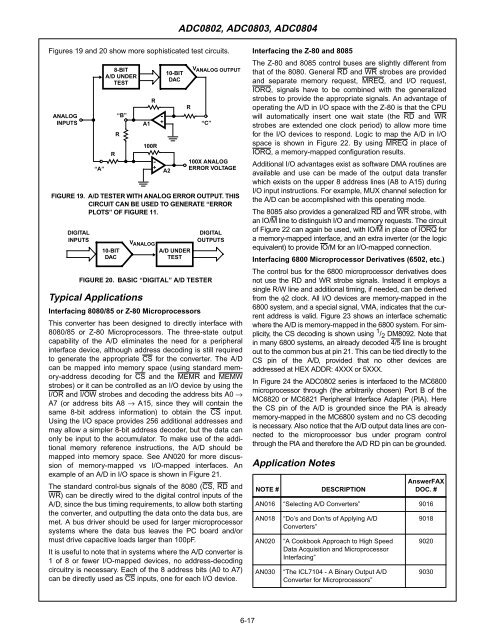
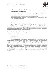
ADC0802, ADC0803, ADC0804Figures 19 and 20 show more sophisticated test circuits.ANALOGINPUTS“A”8-BITA/D UNDERTESTTypical ApplicationsR“B”RA1Interfacing 8080/85 or Z-80 MicroprocessorsThis converter has been designed to directly interface with8080/85 or Z-80 Microprocessors. <strong>The</strong> three-state outputcapability of the A/D eliminates the need for a peripheralinterface device, although address decoding is still requiredto generate the appropriate CS for the converter. <strong>The</strong> A/Dcan be mapped into memory space (using standard memory-addressdecoding for CS and the MEMR and MEMWstrobes) or it can be controlled as an I/O device by using theI/OR and I/OW strobes and decoding the address bits A0 →A7 (or address bits A8 → A15, since they will contain thesame 8-bit address information) to obtain the CS input.Using the I/O space provides 256 additional addresses andmay allow a simpler 8-bit address decoder, but the data canonly be input to the accumulator. To make use of the additionalmemory reference instructions, the A/D should bemapped into memory space. See AN020 for more discussionof memory-mapped vs I/O-mapped interfaces. Anexample of an A/D in I/O space is shown in Figure 21.<strong>The</strong> standard control-bus signals of the 8080 (CS, RD andWR) can be directly wired to the digital control inputs of theA/D, since the bus timing requirements, to allow both startingthe converter, and outputting the data onto the data bus, aremet. A bus driver should be used for larger microprocessorsystems where the data bus leaves the PC board and/ormust drive capacitive loads larger than 100pF.It is useful to note that in systems where the A/D converter is1 of 8 or fewer I/O-mapped devices, no address-decodingcircuitry is necessary. Each of the 8 address bits (A0 to A7)can be directly used as CS inputs, one for each I/O device.R100R-+-+10-BITDACA2RV ANALOG OUTPUT“C”100X ANALOGERROR VOLTAGEFIGURE 19. A/D TESTER WITH ANALOG ERROR OUTPUT. THISCIRCUIT CAN BE USED TO GENERATE “ERRORPLOTS” OF FIGURE 11.DIGITALINPUTS10-BITDACV ANALOGA/D UNDERTESTDIGITALOUTPUTSFIGURE 20. BASIC “DIGITAL” A/D TESTERInterfacing the Z-80 and 8085<strong>The</strong> Z-80 and 8085 control buses are slightly different fromthat of the 8080. General RD and WR strobes are providedand separate memory request, MREQ, and I/O request,IORQ, signals have to be combined with the generalizedstrobes to provide the appropriate signals. An advantage ofoperating the A/D in I/O space with the Z-80 is that the CPUwill automatically insert one wait state (the RD and WRstrobes are extended one clock period) to allow more timefor the I/O devices to respond. Logic to map the A/D in I/Ospace is shown in Figure 22. By using MREQ in place ofIORQ, a memory-mapped configuration results.Additional I/O advantages exist as software DMA routines areavailable and use can be made of the output data transferwhich exists on the upper 8 address lines (A8 to A15) duringI/O input instructions. For example, MUX channel selection forthe A/D can be accomplished with this operating mode.<strong>The</strong> 8085 also provides a generalized RD and WR strobe, withan IO/M line to distinguish I/O and memory requests. <strong>The</strong> circuitof Figure 22 can again be used, with IO/M in place of IORQ fora memory-mapped interface, and an extra inverter (or the logicequivalent) to provide IO/M for an I/O-mapped connection.Interfacing 6800 Microprocessor Derivatives (6502, etc.)<strong>The</strong> control bus for the 6800 microprocessor derivatives doesnot use the RD and WR strobe signals. Instead it employs asingle R/W line and additional timing, if needed, can be derivedfrom the φ2 clock. All I/O devices are memory-mapped in the6800 system, and a special signal, VMA, indicates that the currentaddress is valid. Figure 23 shows an interface schematicwhere the A/D is memory-mapped in the 6800 system. For simplicity,the CS decoding is shown using 1 / 2 DM8092. Note thatin many 6800 systems, an already decoded 4/5 line is broughtout to the common bus at pin 21. This can be tied directly to theCS pin of the A/D, provided that no other devices areaddressed at HEX ADDR: 4XXX or 5XXX.In Figure 24 the ADC0802 series is interfaced to the MC6800microprocessor through (the arbitrarily chosen) Port B of theMC6820 or MC6821 Peripheral Interface Adapter (PlA). Herethe CS pin of the A/D is grounded since the PlA is alreadymemory-mapped in the MC6800 system and no CS decodingis necessary. Also notice that the A/D output data lines are connectedto the microprocessor bus under program controlthrough the PlA and therefore the A/D RD pin can be grounded.Application NotesNOTE #DESCRIPTIONAnswerFAXDOC. #AN016 “Selecting A/D Converters” 9016AN018AN020AN030“Do’s and Don’ts of Applying A/DConverters”“A Cookbook Approach to High SpeedData Acquisition and MicroprocessorInterfacing”“<strong>The</strong> ICL7104 - A Binary Output A/DConverter for Microprocessors”9018902090306-17
- Page 1 and 2:
CHAPTER 3METHODOLOGY3.1 OverviewThe
- Page 3 and 4:
3.2.2 Analog To Digital Conversion
- Page 5 and 6:
Figure 3.5: Source Code for Convers
- Page 7 and 8:
3.2.4 Water Monitoring System Circu
- Page 9 and 10:
3.3 Programming.Programming is the
- Page 11 and 12:
ISP flash programmer in Figure 3.11
- Page 13 and 14:
The Visual Basic program will start
- Page 15 and 16:
Distance(cm)ReadingVoltage Trial1 (
- Page 17 and 18:
4.2 Signal ConversionA sensor has s
- Page 19 and 20:
4.3 User InterfaceBased on Table 4.
- Page 21 and 22:
Hardware DesignBasically, the const
- Page 23 and 24:
CHAPTER 5CONCLUSION5.1 SummaryWater
- Page 25 and 26:
This project can be expanded by usi
- Page 27 and 28:
APPENDICES41
- Page 29 and 30:
cjne a,volt,xsamejmp startxsame:mov
- Page 31 and 32: xsame19:jnc more19mov dptr,#XVALIDc
- Page 33 and 34: etrx:jnb ri,$clr rimov a,sbufretdel
- Page 35 and 36: ElseShape8.FillColor = vbWhiteEnd I
- Page 37 and 38: Private Sub Timer3_Timer()Label3.Ca
- Page 39 and 40: APPENDIX EData Sheet AT89S5253
- Page 41 and 42: Features• Compatible with MCS-51
- Page 43 and 44: AT89S52Block DiagramP0.0 - P0.7P2.0
- Page 45 and 46: AT89S52weakly pulled high. Setting
- Page 47 and 48: AT89S52Table 3a. AUXR: Auxiliary Re
- Page 49 and 50: AT89S52Watchdog Timer(One-time Enab
- Page 51 and 52: AT89S52Figure 6. Timer 2 Auto Reloa
- Page 53 and 54: AT89S52Baud Rate GeneratorTimer 2 i
- Page 55 and 56: AT89S52Oscillator CharacteristicsXT
- Page 57 and 58: AT89S52frequency should be less tha
- Page 59 and 60: Figure 15. Flash Programming and Ve
- Page 61 and 62: AT89S52Table 9. Serial Programming
- Page 63 and 64: AT89S52Absolute Maximum Ratings*Ope
- Page 65 and 66: AT89S52External Program Memory Read
- Page 67 and 68: AT89S52Serial Port Timing: Shift Re
- Page 69 and 70: Packaging Information44A, 44-lead,
- Page 71 and 72: August 1997SemiconductorADC0802, AD
- Page 73 and 74: ADC0802, ADC0803, ADC0804Absolute M
- Page 75 and 76: ADC0802, ADC0803, ADC0804Electrical
- Page 77 and 78: ADC0802, ADC0803, ADC0804Typical Pe
- Page 79 and 80: ADC0802, ADC0803, ADC0804The device
- Page 81: ADC0802, ADC0803, ADC0804V IN ±5VR
- Page 85 and 86: ADC0802, ADC0803, ADC0804IRQ (4)†