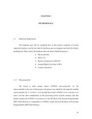
CHAPTER 3 METHODOLOGY 3.1 Overview The Water Monitoring ...
CHAPTER 3 METHODOLOGY 3.1 Overview The Water Monitoring ...
CHAPTER 3 METHODOLOGY 3.1 Overview The Water Monitoring ...

Create successful ePaper yourself
Turn your PDF publications into a flip-book with our unique Google optimized e-Paper software.
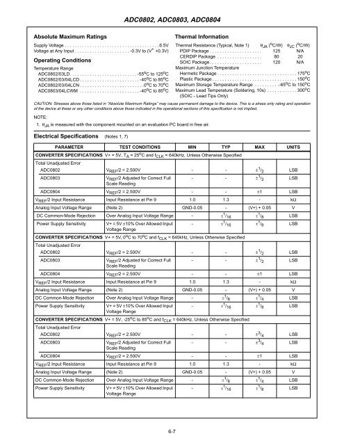
ADC0802, ADC0803, ADC0804Absolute Maximum RatingsSupply Voltage . . . . . . . . . . . . . . . . . . . . . . . . . . . . . . . . . . . . . . 6.5VVoltage at Any Input . . . . . . . . . . . . . . . . . . . . . . -0.3V to (V + +0.3V)Operating ConditionsTemperature RangeADC0802/03LD. . . . . . . . . . . . . . . . . . . . . . . . . . . -55 o C to 125 o CADC0802/03/04LCD . . . . . . . . . . . . . . . . . . . . . . . . -40 o C to 85 o CADC0802/03/04LCN . . . . . . . . . . . . . . . . . . . . . . . . . .0 o C to 70 o CADC0803/04LCWM . . . . . . . . . . . . . . . . . . . . . . . . -40 o C to 85 o C<strong>The</strong>rmal Information<strong>The</strong>rmal Resistance (Typical, Note 1) θ JA ( o C/W) θ JC ( o C/W)PDIP Package . . . . . . . . . . . . . . . . . . . . . 125 N/ACERDIP Package . . . . . . . . . . . . . . . . . . 80 20SOIC Package . . . . . . . . . . . . . . . . . . . . . 120 N/AMaximum Junction TemperatureHermetic Package . . . . . . . . . . . . . . . . . . . . . . . . . . . . . . . . 175 o CPlastic Package . . . . . . . . . . . . . . . . . . . . . . . . . . . . . . . . . . 150 o CMaximum Storage Temperature Range . . . . . . . . . .-65 o C to 150 o CMaximum Lead Temperature (Soldering, 10s) . . . . . . . . . . . . 300 o C(SOIC - Lead Tips Only)CAUTION: Stresses above those listed in “Absolute Maximum Ratings” may cause permanent damage to the device. This is a stress only rating and operationof the device at these or any other conditions above those indicated in the operational sections of this specification is not implied.NOTE:1. θ JA is measured with the component mounted on an evaluation PC board in free air.Electrical Specifications (Notes 1, 7)PARAMETER TEST CONDITIONS MIN TYP MAX UNITSCONVERTER SPECIFICATIONS V+ = 5V, T A = 25 o C and f CLK = 640kHz, Unless Otherwise SpecifiedTotal Unadjusted ErrorADC0802 V REF /2 = 2.500V - - ± 1 / 2 LSBADC0803V REF /2 Adjusted for Correct FullScale Reading- - ± 1 / 2 LSBADC0804 V REF /2 = 2.500V - - ±1 LSBV REF /2 Input Resistance Input Resistance at Pin 9 1.0 1.3 - kΩAnalog Input Voltage Range (Note 2) GND-0.05 - (V+) + 0.05 VDC Common-Mode Rejection Over Analog Input Voltage Range - ± 1 / 16 ± 1 / 8 LSBPower Supply Sensitivity V+ = 5V ±10% Over Allowed InputVoltage Range- ± 1 / 16 ± 1 / 8 LSBCONVERTER SPECIFICATIONS V+ = 5V, 0 o C to 70 o C and f CLK = 640kHz, Unless Otherwise SpecifiedTotal Unadjusted ErrorADC0802 V REF /2 = 2.500V - - ± 1 / 2 LSBADC0803V REF /2 Adjusted for Correct FullScale Reading- - ± 1 / 2 LSBADC0804 V REF /2 = 2.500V - - ±1 LSBV REF /2 Input Resistance Input Resistance at Pin 9 1.0 1.3 - kΩAnalog Input Voltage Range (Note 2) GND-0.05 - (V+) + 0.05 VDC Common-Mode Rejection Over Analog Input Voltage Range - ± 1 / 8 ± 1 / 4 LSBPower Supply Sensitivity V+ = 5V ±10% Over Allowed InputVoltage Range- ± 1 / 16 ± 1 / 8 LSBCONVERTER SPECIFICATIONS V+ = 5V, -25 o C to 85 o C and f CLK = 640kHz, Unless Otherwise SpecifiedTotal Unadjusted ErrorADC0802 V REF /2 = 2.500V - - ± 3 / 4 LSBADC0803V REF /2 Adjusted for Correct FullScale Reading- - ± 3 / 4 LSBADC0804 V REF /2 = 2.500V - - ±1 LSBV REF /2 Input Resistance Input Resistance at Pin 9 1.0 1.3 - kΩAnalog Input Voltage Range (Note 2) GND-0.05 - (V+) + 0.05 VDC Common-Mode Rejection Over Analog Input Voltage Range - ± 1 / 8 ± 1 / 4 LSBPower Supply Sensitivity V+ = 5V ±10% Over Allowed InputVoltage Range- ± 1 / 16 ± 1 / 8 LSB6-7