CHAPTER 3 METHODOLOGY 3.1 Overview The Water Monitoring ...
CHAPTER 3 METHODOLOGY 3.1 Overview The Water Monitoring ...
CHAPTER 3 METHODOLOGY 3.1 Overview The Water Monitoring ...

You also want an ePaper? Increase the reach of your titles
YUMPU automatically turns print PDFs into web optimized ePapers that Google loves.
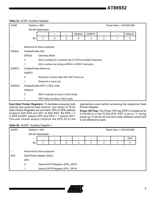
AT89S52Table 3a. AUXR: Auxiliary RegisterAUXR Address = 8EH Reset Value = XXX00XX0BNot Bit Addressable– – – WDIDLE DISRTO – – DISALEBit 7 6 5 4 3 2 1 0– Reserved for future expansionDISALEDisable/Enable ALEDISALEOperating Mode0 ALE is emitted at a constant rate of 1/6 the oscillator frequency1 ALE is active only during a MOVX or MOVC instructionDISRTODisable/Enable Reset outDISRTO0 Reset pin is driven High after WDT times out1 Reset pin is input onlyWDIDLEDisable/Enable WDT in IDLE modeWDIDLE0 WDT continues to count in IDLE mode1 WDT halts counting in IDLE modeDual Data Pointer Registers: To facilitate accessing bothinternal and external data memory, two banks of 16-bitData Pointer Registers are provided: DP0 at SFR addresslocations 82H-83H and DP1 at 84H-85H. Bit DPS = 0in SFR AUXR1 selects DP0 and DPS = 1 selects DP1.<strong>The</strong> user should always initialize the DPS bit to theappropriate value before accessing the respective DataPointer Register.Power Off Flag: <strong>The</strong> Power Off Flag (POF) is located at bit4 (PCON.4) in the PCON SFR. POF is set to “1” duringpower up. It can be set and rest under software control andis not affected by reset.Table 3b. AUXR1: Auxiliary Register 1AUXR1 Address = A2H Reset Value = XXXXXXX0BNot Bit Addressable– – – – – – – DPSBit 7 6 5 4 3 2 1 0– Reserved for future expansionDPSData Pointer Register SelectDPS0 Selects DPTR Registers DP0L, DP0H1 Selects DPTR Registers DP1L, DP1H7