XILINX VIRTEX-II SERIES FPGAs http://www.xilinx.com/products/platform/ Product Selection Matrix Clock CLB Resources Memory Resources DSP Resources I/O Features Speed Virtex-II Series EasyPath Solution (see note 4) PowerPC Processor Blocks RocketIO Transceiver Blocks Configuration Memory (Bits) Platform Flash PROM Industrial Speed Grades (slowest to fastest) Commercial Speed Grades (slowest to fastest) I/O Standards Maximum I/O Maximum Differential I/O Pairs Digitally Controlled Impedance # DCM Blocks (see Note 3) DCM Frequency (min/max) # 18x18 Dedicated Multipliers Total Block RAM (kbits) # 18 kbits Block RAM Max. Distributed RAM Bits (kbits) CLB Flip-Flops Logic Cells (see note 2) Number of Slices CLB Array (Row x Col) System Gates (see note 1) XC2VP2 * 16 x 22 1,408 3,168 2816 44 12 216 12 24/420 4 YES 100 204 LDT-25, LVDS-25, LVDSEXT-25, -5 -6 -7 -5 -6 1.31M 4 0 BLVDS-25, ULVDS-25, LVPECL-25, XC2VP4 40 x 22 3,008 6,768 6,016 94 28 504 28 24/420 4 YES 172 348 -5 -6 -7 -5 -6 3.01M 4 1 LVCMOS25, LVCMOS18, XC2VP7 * 40 x 34 4,928 11,088 9,856 154 44 792 44 24/420 4 YES 196 396 LVCMOS15, PCI33, LVTTL, -5 -6 -7 -5 -6 4.49M 8 1 LVCMOS33, PCI-X, PCI66, GTL, XC2VP20 * 56 x 46 9,280 20,880 18,560 290 88 1,584 88 24/420 8 YES 276 564 -5 -6 -7 -5 -6 8.21M 8 2 GTL+, HSTL I (1.5V,1.8V), XC2VP30 HSTL II (1.5V,1.8V), HSTL III (1.5V,1.8V), HSTL IV (1.5V,1.8V), SSTL2I, SSTL2II, SSTL18 I, SSTL18 II 3 * 80 x 46 13,696 30,816 27,392 428 136 2448 136 24/420 8 YES 372 644 -5 -6 -7 -5 -6 11.36M 8 2 XC2VP403 * 88 x 58 19,392 43,632 38,784 606 192 3,456 192 24/420 8 YES 396 804 -5 -6 -7 -5 -6 15.56M 0** or 12 2 XC2VP503 Virtex-II Pro Family – 1.5 Volt * 88 x 70 23,616 53,136 47,232 738 232 4,176 232 24/420 8 YES 420 852 -5 -6 -7 -5 -6 19.02M 0** or 16 2 ✔ ✔ ✔ ✔ ✔ ✔ ISP ISP System ACE ISP XC2VP70 3 * 104 x 82 33,088 74,448 66,176 1,034 328 5,904 328 24/420 8 YES 492 996 -5 -6 -7 -5 -6 25.60M 16 or 20 2 XC2VP100 3 * 120 x 94 44,096 99,216 88,192 1,378 444 7,992 444 24/420 12 YES 572 1,164 -5 -6 -7 -5 -6 33.65M 0** or 20 2 XC2VP125 3 * 136 x 106 55,616 125,136 111,232 1,738 556 10,008 556 24/420 12 YES 644 1,200 -5 -6 -7 -5 -6 42.78M 0**, 20 or 24 2 Virtex-II Family – 1.5 Volt XC2V40 40K 8 x 8 256 576 512 8 4 72 4 24/420 4 YES 44 88 LDT-25, LVPECL-33, -4 -5 -6 -4 -5 0.4M – – LVDS-33, LVDS-25, XC2V80 80K 16 x 8 512 1,152 1,024 16 8 144 8 24/420 4 YES 60 120 LVDSEXT-33, LVDSEXT-25, -4 -5 -6 -4 -5 0.6M – – XC2V250 250K 24 x 16 1,536 3,456 3,072 48 24 432 24 24/420 8 YES 100 200 BLVDS-25, ULVDS-25, -4 -5 -6 -4 -5 1.7M – – LVTTL, LVCMOS33, XC2V500 500K 32 x 24 3,072 6,912 6,144 96 32 576 32 24/420 8 YES 132 264 LVCMOS25, LVCMOS18, -4 -5 -6 -4 -5 2.8M – – LVCMOS15, PCI33, PCI66, XC2V1000 1M 40 x 32 5,120 11,520 10,240 160 40 720 40 24/420 8 YES 216 432 PCI-X, GTL, GTL+, HSTL I, -4 -5 -6 -4 -5 4.1M – – XC2V1500 1.5M 48 x 40 7,680 17,280 15,360 240 48 864 48 24/420 8 YES 264 528 HSTL II, HSTL III, HSTL IV, -4 -5 -6 -4 -5 5.7M – – SSTL2I, SSTL2II, SSTL3 I, XC2V2000 2M 56 x 48 10,752 24,192 21,504 336 56 1,008 56 24/420 8 YES 312 624 SSTL3 II, AGP, AGP-2X -4 -5 -6 -4 -5 7.5M – – Platform FPGAs ISP ✔ ✔ ✔ ✔ XC2V3000 3 3M 64 x 56 14,336 32,256 28,672 448 96 1,728 96 24/420 12 YES 360 720 -4 -5 -6 -4 -5 10.5M – – XC2V4000 3 4M 80 x 72 23,040 51,840 46,080 720 120 2,160 120 24/420 12 YES 456 912 -4 -5 -6 -4 -5 15.7M – – XC2V6000 3 6M 96 x 88 33,792 76,032 67,584 1,056 144 2,592 144 24/420 12 YES 552 1,104 -4 -5 -6 -4 -5 21.9M – – 8M 112 x 104 46,592 104,832 93,184 1,456 168 3,024 168 24/420 12 YES 554 1,108 -4 -5 -4 -5 29.1M – – XC2V8000 3 * Logic cell counts are a more meaningful measurement of density for the Virtex-II Pro family since system gate count does not take into consideration the benefits of the immersed special blocks such as PowerPC processors and multi-gigabit transceivers. ** RocketIO unavailable in this package. Notes: 1. System Gates include 20-30% of CLBs used as RAM 2. Logic cell = One 4-Input Look Up Table (LUT) + Flip Flop + Carry Logic. 3. DCM = Digital Clock Management 4. Virtex-II Series EasyPath solution available to provide a no risk, no effort cost reduction path for volume production 86 Xcell Journal Fall 2003 Important: Verify all data in this document with the device data sheets found at http://www.xilinx.com/partinfo/databook.htm
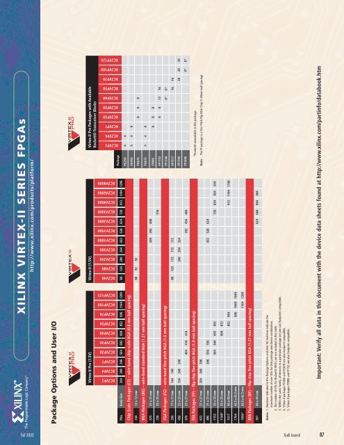
XILINX VIRTEX-II SERIES FPGAs http://www.xilinx.com/products/platform/ Package Options and User I/O Virtex-II Pro Packages with Available RocketIO Transceiver Blocks Virtex-II (1.5V) Virtex-II Pro (1.5V) XC2VP125 XC2VP100 XC2VP70 XC2VP50 XC2VP40 XC2VP30 XC2VP20 XC2VP7 XC2VP4 XC2VP2 XC2V8000 XC2V6000 XC2V4000 XC2V3000 XC2V2000 XC2V1500 XC2V1000 XC2V500 XC2V250 XC2V80 XC2V40 XC2VP125 XC2VP100 XC2VP70 XC2VP50 XC2VP40 XC2VP30 XC2VP20 XC2VP7 XC2VP4 XC2VP2 Package 1296 1104 912 720 624 528 432 264 200 120 88 1200 1164 996 852 804 692 564 396 348 204 Pins Body Size FG256 4 4 FG456 4 4 8 Chip Scale Packages (CS) – wire-bond chip-scale BGA (0.8 mm ball spacing) FG676 8 8 8 88 92 92 144 12 x 12 mm FG672 4 4 8 BGA Packages (BG) – wire-bond standard BGA (1.27 mm ball spacing) 328 392 408 575 31 x 31 mm FF896 8 8 8 FF1152 8 8 12 16 516 728 35 x 35 mm FF1148 0* 0* FGA Packages (FG) – wire-bond fine-pitch BGA (1.0 mm ball spacing) FF1517 16 16 140 140 88 120 172 172 172 256 17 x 17 mm FF1704 20 20 24 FF1696 0* 0* 156 248 248 200 264 324 456 23 x 23 mm 404 416 416 392 456 484 676 27 x 27 mm *RocketIO unavailable in this package. FFA Packages (FF) – flip-chip fine-pitch BGA (1.0 mm ball spacing) The FF package is a Fine Pitch Flip BGA Chip (1.00mm ball spacing). Note: 204 348 396 672 27 x 27 mm 396 556 556 432 528 624 896 31 x 31 mm 564 644 692 692 720 824 824 824 1152 35 x 35 mm 804 812 1148* 35 x 35 mm 852 964 912 1104 1108 1517 40 x 40 mm 996 1040 1040 1704 42.5 x 42.5 mm 1164 1200 1696* 42.5 x 42.5 mm BFA Packages (BF) – flip-chip fine-pitch BGA (1.27 mm ball spacing) 624 684 684 684 40 x 40 mm 957 Notes: 1. Numbers indicated in the Package Options and User I/O matrices indicate the maximum number of user I/Os for that package and device combination. 2. The number of I/Os for RocketIO MGTs are not included in this table. 3. Within the same family, all devices in a particular package are pin-out (footprint) compatible. 4. Virtex-II packages FG456 and FG676 are also footprint compatible. 5. Virtex-II packages FF896 and FF152 are also footprint compatible. Fall 2003 Xcell Journal 87 Important: Verify all data in this document with the device data sheets found at http://www.xilinx.com/partinfo/databook.htm
- Page 1 and 2:
ISSUE 47, FALL 2003 XCELL JOURNAL X
- Page 3 and 4:
EDITOR IN CHIEF Carlis Collins edit
- Page 5 and 6:
View from the top Innovation, Educa
- Page 7 and 8:
High Density Spartan-3 Support ISE
- Page 9 and 10:
compilation block from the XtremeDS
- Page 11 and 12:
Get Physical with the PALACE Synthe
- Page 13 and 14:
You can control PALACE operations i
- Page 15 and 16:
Integration of Functions Glue Logic
- Page 17 and 18:
4. Support for Xilinx V2PDK Softwar
- Page 19 and 20:
Resulting PAR Fmax LUT Count 135 12
- Page 21 and 22:
points. The ability to support many
- Page 23 and 24:
Get the Platform Flash PROMise Redu
- Page 25 and 26:
implemented. This means that there
- Page 27 and 28:
• Synchronizing Logic - At this s
- Page 29 and 30:
64 Light Sensors LOAD Although this
- Page 31 and 32:
The DQS net could potentially be de
- Page 33 and 34:
Design Security Consider the philos
- Page 35 and 36: Bitstream Encryption Simple Encrypt
- Page 37 and 38: System Challenges The differing req
- Page 39 and 40: nVisage captures it all As a profes
- Page 41 and 42: A unique, scientific research instr
- Page 43 and 44: utes, and seconds, the “counter a
- Page 45 and 46: cisely 0-1-0-1, the cell’s fitnes
- Page 47 and 48: y Liza Boland System Architect, Con
- Page 49 and 50: team plans to migrate to a more com
- Page 51 and 52: ands on the market. We use a 73.768
- Page 53 and 54: Boeing Harnesses Virtex-II Pro Plat
- Page 55 and 56: straints make it very hard for embe
- Page 57 and 58: oss The Board. Avnet Design Servic
- Page 59 and 60: To give you a good jump-start on de
- Page 61 and 62: Develop Applications Right Out of t
- Page 63 and 64: • Two HSSDC2 connectors for imple
- Page 65 and 66: y Jim Beneke Director of Technical
- Page 67 and 68: User Application and Bluetooth Prot
- Page 69 and 70: from one fabrication line to anothe
- Page 71 and 72: Take the Titanium Solution Xilinx T
- Page 73 and 74: Support and Titanium Technical Serv
- Page 75: Celoxica, IBM, Mentor Graphics, Nal
- Page 78 and 79: Xilinx AllianceCORE Third-Party IP
- Page 80 and 81: XPERTS Partners 3T BV www.3T.nl/ De
- Page 82 and 83: Mikrokrets AS www.mikrokrets.no/ FP
- Page 85: XILINX CPLD http://www.xilinx.com/p
- Page 89 and 90: XILINX SPARTAN FPGAs http://www.xil
- Page 91 and 92: XILINX CONFIGURATION STORAGE SOLUTI
- Page 93 and 94: XILINX IP REFERENCE GUIDE Function
- Page 95 and 96: XILINX IP REFERENCE GUIDE Function
- Page 97 and 98: XILINX IP REFERENCE GUIDE Function
- Page 99 and 100: Avoid messy timing mistakes. Use Me