VS1033 - MP3/AAC/WMA/MIDI AUDIO CODEC - VLSI Solution
VS1033 - MP3/AAC/WMA/MIDI AUDIO CODEC - VLSI Solution
VS1033 - MP3/AAC/WMA/MIDI AUDIO CODEC - VLSI Solution

You also want an ePaper? Increase the reach of your titles
YUMPU automatically turns print PDFs into web optimized ePapers that Google loves.
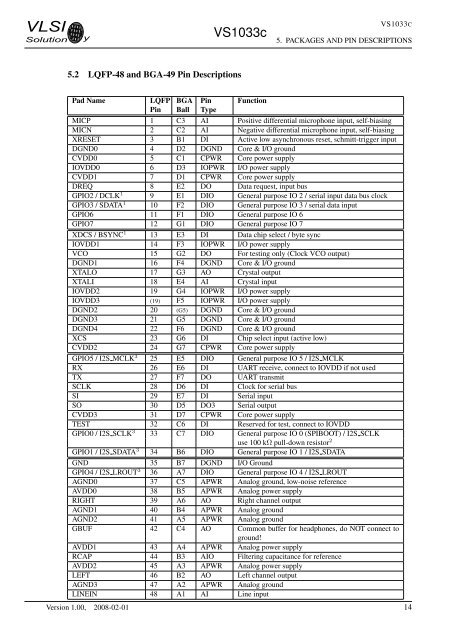
<strong>VLSI</strong><strong>Solution</strong> y<strong>VS1033</strong>c<strong>VS1033</strong>C5. PACKAGES AND PIN DESCRIPTIONS5.2 LQFP-48 and BGA-49 Pin DescriptionsPad NameLQFPPinBGABallPinTypeFunctionMICP 1 C3 AI Positive differential microphone input, self-biasingMICN 2 C2 AI Negative differential microphone input, self-biasingXRESET 3 B1 DI Active low asynchronous reset, schmitt-trigger inputDGND0 4 D2 DGND Core & I/O groundCVDD0 5 C1 CPWR Core power supplyIOVDD0 6 D3 IOPWR I/O power supplyCVDD1 7 D1 CPWR Core power supplyDREQ 8 E2 DO Data request, input busGPIO2 / DCLK 1 9 E1 DIO General purpose IO 2 / serial input data bus clockGPIO3 / SDATA 1 10 F2 DIO General purpose IO 3 / serial data inputGPIO6 11 F1 DIO General purpose IO 6GPIO7 12 G1 DIO General purpose IO 7XDCS / BSYNC 1 13 E3 DI Data chip select / byte syncIOVDD1 14 F3 IOPWR I/O power supplyVCO 15 G2 DO For testing only (Clock VCO output)DGND1 16 F4 DGND Core & I/O groundXTALO 17 G3 AO Crystal outputXTALI 18 E4 AI Crystal inputIOVDD2 19 G4 IOPWR I/O power supplyIOVDD3 (19) F5 IOPWR I/O power supplyDGND2 20 (G5) DGND Core & I/O groundDGND3 21 G5 DGND Core & I/O groundDGND4 22 F6 DGND Core & I/O groundXCS 23 G6 DI Chip select input (active low)CVDD2 24 G7 CPWR Core power supplyGPIO5 / I2S MCLK 3 25 E5 DIO General purpose IO 5 / I2S MCLKRX 26 E6 DI UART receive, connect to IOVDD if not usedTX 27 F7 DO UART transmitSCLK 28 D6 DI Clock for serial busSI 29 E7 DI Serial inputSO 30 D5 DO3 Serial outputCVDD3 31 D7 CPWR Core power supplyTEST 32 C6 DI Reserved for test, connect to IOVDDGPIO0 / I2S SCLK 3 33 C7 DIO General purpose IO 0 (SPIBOOT) / I2S SCLKuse 100 kΩ pull-down resistor 2GPIO1 / I2S SDATA 3 34 B6 DIO General purpose IO 1 / I2S SDATAGND 35 B7 DGND I/O GroundGPIO4 / I2S LROUT 3 36 A7 DIO General purpose IO 4 / I2S LROUTAGND0 37 C5 APWR Analog ground, low-noise referenceAVDD0 38 B5 APWR Analog power supplyRIGHT 39 A6 AO Right channel outputAGND1 40 B4 APWR Analog groundAGND2 41 A5 APWR Analog groundGBUF 42 C4 AO Common buffer for headphones, do NOT connect toground!AVDD1 43 A4 APWR Analog power supplyRCAP 44 B3 AIO Filtering capacitance for referenceAVDD2 45 A3 APWR Analog power supplyLEFT 46 B2 AO Left channel outputAGND3 47 A2 APWR Analog groundLINEIN 48 A1 AI Line inputVersion 1.00, 2008-02-01 14