Design, Fabrication and Characterization of a Microwave Resonator ...
Design, Fabrication and Characterization of a Microwave Resonator ...
Design, Fabrication and Characterization of a Microwave Resonator ...

Create successful ePaper yourself
Turn your PDF publications into a flip-book with our unique Google optimized e-Paper software.
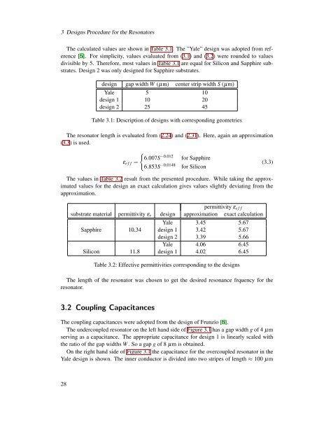
3 <strong>Design</strong>s Procedure for the <strong>Resonator</strong>sThe calculated values are shown in Table 3.1. The ”Yale” design was adopted from reference[6]. For simplicity, values evaluated from (3.1) <strong>and</strong> (3.2) were rounded to valuesdivisible by 5. Therefore, most values in Table 3.1 are equal for Silicon <strong>and</strong> Sapphire substrates.<strong>Design</strong> 2 was only designed for Sapphire substrates.design gap width W (µm) center strip width S (µm)Yale 5 10design 1 10 20design 2 25 45Table 3.1: Description <strong>of</strong> designs with corresponding geometriesThe resonator length is evaluated from (2.24) <strong>and</strong> (2.31). Here, again an approximation(3.3) is used.ε e f f ={6.007S −0.012 for Sapphire6.853S −0.0148 for Silicon(3.3)The values in Table 3.2 result from the presented procedure. While taking the approximatedvalues for the design an exact calculation gives values slightly deviating from theapproximation.permittivity ε e f fsubstrate material permittivity ε r design approximation exact calculationYale 3.45 5.67Sapphire 10.34 design 1 3.42 5.67design 2 3.39 5.66Yale 4.06 6.45Silicon 11.8 design 1 4.02 6.45Table 3.2: Effective permittivities corresponding to the designsThe length <strong>of</strong> the resonator was chosen to get the desired resonance frquency for theresonator.3.2 Coupling CapacitancesThe coupling capacitances were adopted from the design <strong>of</strong> Frunzio [6].The undercoupled resonator on the left h<strong>and</strong> side <strong>of</strong> Figure 3.1 has a gap width g <strong>of</strong> 4 µmserving as a capacitance. The appropriate capacitance for design 1 is linearly scaled withthe ratio <strong>of</strong> the gap widths W. So a gap g <strong>of</strong> 8 µm is obtained.On the right h<strong>and</strong> side <strong>of</strong> Figure 3.1 the capacitance for the overcoupled resonator in theYale design is shown. The inner conductor is divided into two stripes <strong>of</strong> length ≈ 100 µm28