Design, Fabrication and Characterization of a Microwave Resonator ...
Design, Fabrication and Characterization of a Microwave Resonator ...
Design, Fabrication and Characterization of a Microwave Resonator ...

You also want an ePaper? Increase the reach of your titles
YUMPU automatically turns print PDFs into web optimized ePapers that Google loves.
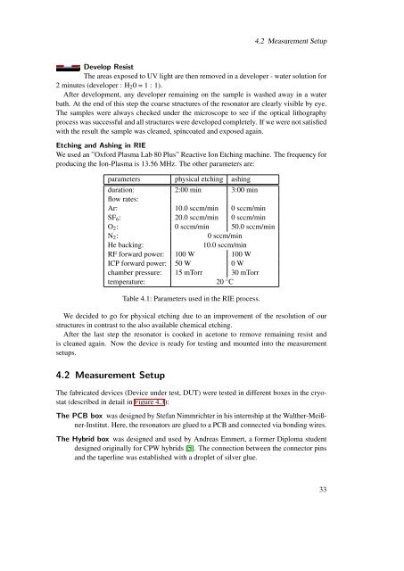
4.2 Measurement SetupDevelop ResistThe areas exposed to UV light are then removed in a developer - water solution for2 minutes (developer : H 2 0 = 1 : 1).After development, any developer remaining on the sample is washed away in a waterbath. At the end <strong>of</strong> this step the coarse structures <strong>of</strong> the resonator are clearly visible by eye.The samples were always checked under the microscope to see if the optical lithographyprocess was successful <strong>and</strong> all structures were developed completely. If we were not satisfiedwith the result the sample was cleaned, spincoated <strong>and</strong> exposed again.Etching <strong>and</strong> Ashing in RIEWe used an ”Oxford Plasma Lab 80 Plus” Reactive Ion Etching machine. The frequency forproducing the Ion-Plasma is 13.56 MHz. The other parameters are:parameters physical etching ashingduration: 2:00 min 3:00 minflow rates:Ar: 10.0 sccm/min 0 sccm/minSF 6 : 20.0 sccm/min 0 sccm/minO 2 : 0 sccm/min 50.0 sccm/minN 2 :0 sccm/minHe backing:10.0 sccm/minRF forward power: 100 W 100 WICP forward power: 50 W 0 Wchamber pressure: 15 mTorr 30 mTorrtemperature:20 ◦ CTable 4.1: Parameters used in the RIE process.We decided to go for physical etching due to an improvement <strong>of</strong> the resolution <strong>of</strong> ourstructures in contrast to the also available chemical etching.After the last step the resonator is cooked in acetone to remove remaining resist <strong>and</strong>is cleaned again. Now the device is ready for testing <strong>and</strong> mounted into the measurementsetups.4.2 Measurement SetupThe fabricated devices (Device under test, DUT) were tested in different boxes in the cryostat(described in detail in Figure 4.3):The PCB box was designed by Stefan Nimmrichter in his internship at the Walther-Meißner-Institut.Here, the resonators are glued to a PCB <strong>and</strong> connected via bonding wires.The Hybrid box was designed <strong>and</strong> used by Andreas Emmert, a former Diploma studentdesigned originally for CPW hybrids [5]. The connection between the connector pins<strong>and</strong> the taperline was established with a droplet <strong>of</strong> silver glue.33