(a) 100 µm - Helmholtz-Zentrum Berlin
(a) 100 µm - Helmholtz-Zentrum Berlin
(a) 100 µm - Helmholtz-Zentrum Berlin

You also want an ePaper? Increase the reach of your titles
YUMPU automatically turns print PDFs into web optimized ePapers that Google loves.
122 Discussion<br />
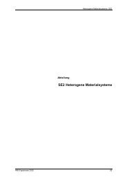
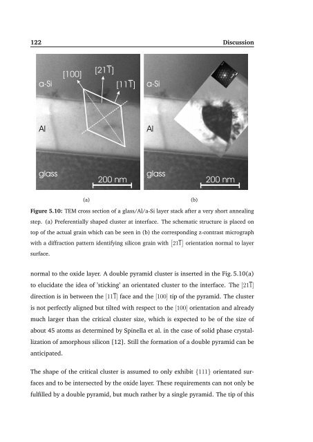
(a) (b)<br />
Figure 5.10: TEM cross section of a glass/Al/a-Si layer stack after a very short annealing<br />
step. (a) Preferentially shaped cluster at interface. The schematic structure is placed on<br />
top of the actual grain which can be seen in (b) the corresponding z-contrast micrograph<br />
with a diffraction pattern identifying silicon grain with � 211 � orientation normal to layer<br />
surface.<br />
normal to the oxide layer. A double pyramid cluster is inserted in the Fig. 5.10(a)<br />
to elucidate the idea of ’sticking’ an orientated cluster to the interface. The [211]<br />
direction is in between the [111] face and the [<strong>100</strong>] tip of the pyramid. The cluster<br />
is not perfectly aligned but tilted with respect to the [<strong>100</strong>] orientation and already<br />
much larger than the critical cluster size, which is expected to be of the size of<br />
about 45 atoms as determined by Spinella et al. in the case of solid phase crystal-<br />
lization of amorphous silicon [12]. Still the formation of a double pyramid can be<br />
anticipated.<br />
The shape of the critical cluster is assumed to only exhibit {111} orientated sur-<br />
faces and to be intersected by the oxide layer. These requirements can not only be<br />
fulfilled by a double pyramid, but much rather by a single pyramid. The tip of this