(a) 100 µm - Helmholtz-Zentrum Berlin
(a) 100 µm - Helmholtz-Zentrum Berlin
(a) 100 µm - Helmholtz-Zentrum Berlin

You also want an ePaper? Increase the reach of your titles
YUMPU automatically turns print PDFs into web optimized ePapers that Google loves.
18 State of the art<br />
Combining this effect of metals on semiconductors and the idea of solid phase<br />
crystallization it was found that metals in contact with amorphous silicon strongly<br />
reduce the crystallization time and temperature. Two microscopic models were<br />
suggested explaining the observed effect. Hiraki [30, 31] deposited monolayers<br />
of gold on amorphous silicon. He found that only upon depositing four monolay-<br />
ers or more crystallization was enhanced. He concluded that some type of bulk<br />
metal must be formed. The bulk is needed because a free electron gas needs to be<br />
formed. The wave function of the free electron gas extends into the amorphous sil-<br />
icon screening the covalent Si bonds. The screened bonds are weakened and thus<br />
crystallization is faster. Tu [32] suggested an interstitial model for near-noble tran-<br />
sition metals. Such metals lack one electron to achieve noble gas configuration. If<br />
such a metal atom would be inserted in an interstitial position of the Si lattice an<br />
electron from the covalent bonds surrounding this atom would be transferred to<br />
the metal. This weakens the bonds around it, enhancing crystallization.<br />
In 1972 S.R. Herd [33] compared the influence of different metals on the crystal-<br />
lization temperature of amorphous silicon and germanium. Metals forming sili-<br />
cides (Ni, Pd, Cu) are distinguished from eutectic metal-silicon systems (Al, Au,<br />
Ag).<br />
Ni in contact with Si forms a NiSi2 phase. The chemical potential for Ni is lower at<br />
the NiSi2/a-Si interface than at the NiSi2/c-Si, thus Ni diffuses to the a-Si side. At<br />
the same time Si diffuses in the opposite direction. This makes the silicide phase<br />
move through the a-Si silicon and leaves crystalline silicon behind. Depending on<br />
the growth parameters the silicide phase either moves anisotropically leading to<br />
needle-like crystallites or isotropically leading to disk-like grains [34]. MIC allows<br />
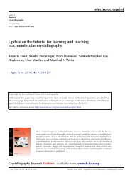
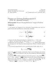
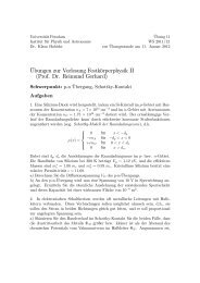
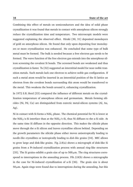
to grow large and disk-like grains. Fig. 2.8(a) shows a micrograph of disk-like Si<br />
grains from a Pt-induced crystallization process with annual ring-like structures<br />
[35]. The Si grains exhibit a grain size of up to 500 <strong>µm</strong>. The ring structures corre-<br />
spond to interruptions in the annealing process. Fib. 2.8(b) shows a micrographs<br />
in the case for Ni-induced crystallization of a-Si [36]. The grain size is about<br />
50 <strong>µm</strong>. Again rings were found due to interruptions during the annealing, but this