(a) 100 µm - Helmholtz-Zentrum Berlin
(a) 100 µm - Helmholtz-Zentrum Berlin
(a) 100 µm - Helmholtz-Zentrum Berlin

You also want an ePaper? Increase the reach of your titles
YUMPU automatically turns print PDFs into web optimized ePapers that Google loves.
30 State of the art<br />
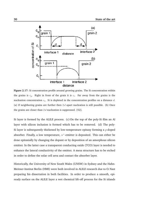
Figure 2.17: Si concentration profile around growing grains. The Si concentration within<br />
the grains is cg. Right in front of the grain it is ci. Far away from the grains is the<br />
nucleation concentration cn. Si is depleted in the concentration profiles on a distance d.<br />
(a) If neighboring grains are further then 2 d apart nucleation is still possible. (b) Once<br />
the grains are closer than 2 d nucleation is suppressed. [52].<br />
Si layer is formed by the ALILE process. (c) On the top of the poly-Si film an Al<br />
layer with silicon inclusion is formed which has to be removed. (d) The poly-<br />
Si layer is subsequently thickened by low-temperature epitaxy forming a p-doped<br />
absorber. Finally, a low temperature, n + -emitter is deposited. This can either be<br />
done epitaxially by changing the dopant or by deposition of an amorphous silicon<br />
emitter. In the latter case a transparent conducting oxide (TCO) layer is needed to<br />
enhance the lateral conductivity of the emitter. A mesa structure has to be etched<br />
in order to define the solar cell area and contact the absorber layer.<br />
Historically, the University of New South Wales (UNSW) in Sydney and the Hahn-<br />
Meitner-Institut <strong>Berlin</strong> (HMI) were both involved in ALILE research due to O. Nast<br />
preparing his dissertation in both facilities. In order to produce a smooth, epi-<br />
ready surface on the ALILE layer a wet chemical lift-off process for the Si islands