(a) 100 µm - Helmholtz-Zentrum Berlin
(a) 100 µm - Helmholtz-Zentrum Berlin
(a) 100 µm - Helmholtz-Zentrum Berlin

Create successful ePaper yourself
Turn your PDF publications into a flip-book with our unique Google optimized e-Paper software.
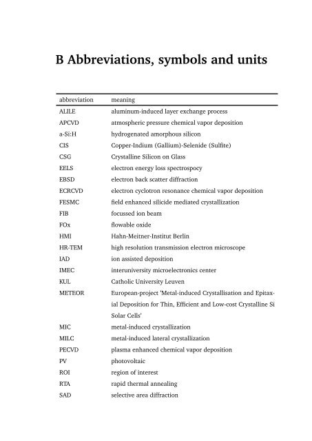
B Abbreviations, symbols and units<br />
abbreviation meaning<br />
ALILE aluminum-induced layer exchange process<br />
APCVD atmospheric pressure chemical vapor deposition<br />
a-Si:H hydrogenated amorphous silicon<br />
CIS Copper-Indium (Gallium)-Selenide (Sulfite)<br />
CSG Crystalline Silicon on Glass<br />
EELS electron energy loss spectrospocy<br />
EBSD electron back scatter diffraction<br />
ECRCVD electron cyclotron resonance chemical vapor deposition<br />
FESMC field enhanced silicide mediated crystallization<br />
FIB focussed ion beam<br />
FOx flowable oxide<br />
HMI Hahn-Meitner-Institut <strong>Berlin</strong><br />
HR-TEM high resolution transmission electron microscope<br />
IAD ion assisted deposition<br />
IMEC interuniversity microelectronics center<br />
KUL Catholic University Leuven<br />
METEOR European-project ’Metal-induced Crystallisation and Epitax-<br />
ial Deposition for Thin, Efficient and Low-cost Crystalline Si<br />
Solar Cells’<br />
MIC metal-induced crystallization<br />
MILC metal-induced lateral crystallization<br />
PECVD plasma enhanced chemical vapor deposition<br />
PV photovoltaic<br />
ROI region of interest<br />
RTA rapid thermal annealing<br />
SAD selective area diffraction