Atomic Layer Deposition (ALD): An Enabler for Nanoscience and ...
Atomic Layer Deposition (ALD): An Enabler for Nanoscience and ...
Atomic Layer Deposition (ALD): An Enabler for Nanoscience and ...

Create successful ePaper yourself
Turn your PDF publications into a flip-book with our unique Google optimized e-Paper software.
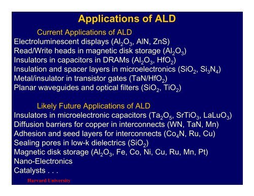
Current Applications of <strong>ALD</strong><br />
Electroluminescent displays (Al 2 O 3 , AlN, ZnS)<br />
Read/Write heads in magnetic disk storage (Al 2 O 3 )<br />
Insulators in capacitors in DRAMs (Al 2 O 3 , HfO 2 )<br />
Insulation <strong>and</strong> spacer layers in microelectronics (SiO 2 , Si 3 N 4 )<br />
Metal/insulator in transistor gates (TaN/HfO 2)<br />
Planar waveguides <strong>and</strong> optical filters (SiO 2 , TiO 2 )<br />
Likely Future Applications of <strong>ALD</strong><br />
Insulators in microelectronic capacitors (Ta 2 O 5 , SrTiO 3 , LaLuO 3 )<br />
Diffusion barriers <strong>for</strong> copper in interconnects (WN, TaN, Mn)<br />
Adhesion <strong>and</strong> seed layers <strong>for</strong> interconnects (Co 4 N, Ru, Cu)<br />
Sealing pores in low-k dielectrics (SiO 2 )<br />
Magnetic disk storage (Al 2 O 3 , Fe, Co, Ni, Cu, Ru, Mn, Pt)<br />
Nano-Electronics<br />
Catalysts . . .<br />
Harvard University<br />
Applications of <strong>ALD</strong>